· AtlasPCB Engineering Team · Engineering · 15 min read
Blind and Buried Via Design Rules for HDI PCB Fabrication
Comprehensive design rules for blind and buried vias in HDI PCB fabrication, covering aspect ratios, drill sizes, annular ring requirements, stacking rules, and DFM guidelines to ensure manufacturability.
Why Via Architecture Defines HDI Manufacturability
High-density interconnect PCB design fundamentally depends on the effective use of blind and buried vias to route signals between layers without consuming precious surface real estate. Unlike through-hole vias that penetrate the entire board thickness, blind and buried vias connect only specific layer pairs, enabling the routing density that modern semiconductor packages demand. However, these via structures impose manufacturing constraints that differ significantly from standard through-hole drilling, and designs that ignore these constraints face rejection at DFM review, yield loss during fabrication, or—worst case—reliability failures in the field.
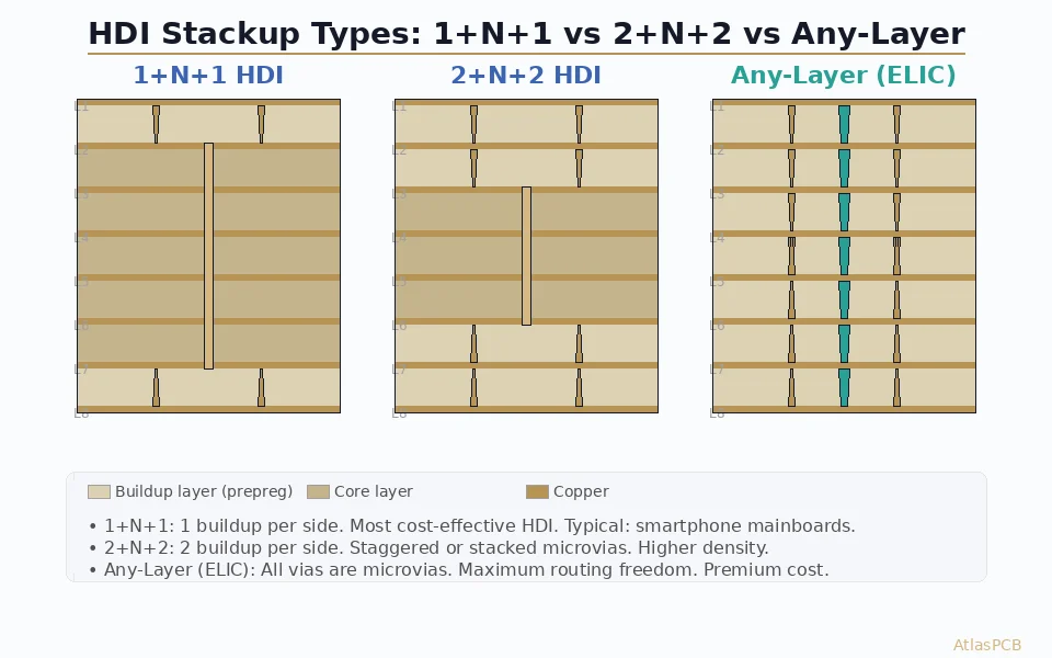
Through years of fabricating HDI boards ranging from simple 1+N+1 structures to complex any-layer designs with stacked microvias, our engineering team has distilled the design rules that consistently produce reliable results. These rules reflect not abstract geometric limits but practical constraints arising from laser drilling physics, plating chemistry, lamination pressures, and reliability testing requirements that every HDI design must satisfy.
Via Types and Their Manufacturing Methods
Understanding the correct design rules requires first understanding how each via type is physically created. The manufacturing method determines the achievable geometry, and designing beyond these physical limits results in either fabrication failure or unreliable structures that pass initial testing but degrade over product life.
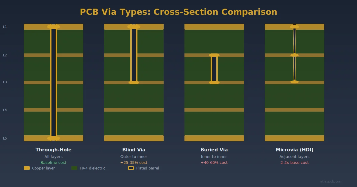
Blind vias connect an outer layer to one or more inner layers without penetrating to the opposite board surface. In HDI construction, these are typically laser-drilled microvias connecting Layer 1 to Layer 2, or in higher-order structures, from Layer 1 through to Layer 3 using a skip via configuration. The laser drilling process—either CO2 or UV laser—ablates the dielectric material to expose the target copper layer, with the copper itself acting as a stop layer that terminates the drill at the correct depth.
Buried vias connect two or more inner layers without reaching either outer surface. These are formed during the sub-lamination stage, drilled mechanically through the inner core before the outer layers are laminated on top. Because they are created before final lamination, buried vias can use conventional mechanical drilling processes, though their aspect ratio is limited by the core thickness they must penetrate.
Microvias represent the most common blind via type in HDI construction. Defined by IPC-2226 as vias with a diameter of 150 micrometers or less with a depth-to-diameter aspect ratio not exceeding 1:1, these laser-drilled features enable the fine-pitch routing that distinguishes HDI from conventional multilayer construction.
Critical Design Rules for Laser-Drilled Blind Microvias
The most common blind via in modern HDI is the laser-drilled microvia connecting adjacent layers. The design rules governing these structures derive from three physical constraints: the laser’s ability to create a clean hole, the plating chemistry’s ability to fill or coat the hole uniformly, and the structure’s ability to survive thermal cycling throughout product life.
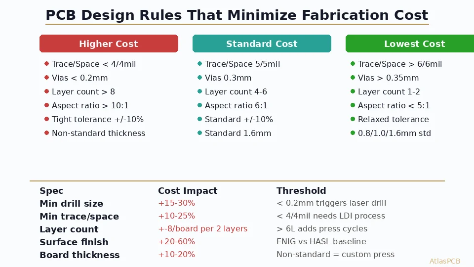
Minimum drill diameter for production laser microvias is 75 micrometers for UV laser systems and 100 micrometers for CO2 laser systems. While laboratories demonstrate smaller features, production environments must maintain this minimum to ensure consistent hole quality across an entire panel. Holes below these limits experience irregular wall profiles, incomplete dielectric removal at the bottom, and difficulty achieving reliable plating coverage. Our standard recommendation for new designs is 100 micrometers minimum, with 75 micrometers available for designs that genuinely require it after engineering review.
Maximum aspect ratio for laser microvias is 1:1, meaning the via depth must not exceed its diameter. For a standard HDI dielectric thickness of 65 to 75 micrometers between layers, this ratio is easily satisfied with minimum drill sizes. However, when designers specify thicker dielectric layers for impedance control purposes or when targeting deeper connections (skip vias), the aspect ratio constraint becomes the limiting factor. A skip via from Layer 1 to Layer 3 spanning 150 micrometers of total dielectric must have a minimum diameter of 150 micrometers to maintain the 1:1 ratio.
Capture pad diameter on the drill entry side must provide adequate annular ring after accounting for drill-to-pad registration tolerance. For laser microvias, the registration between laser drill and pad artwork is typically plus or minus 25 micrometers. With a 100 micrometer drill and 25 micrometer registration tolerance on each side, the minimum capture pad diameter is 200 micrometers to guarantee 25 micrometers of annular ring on all sides under worst-case misregistration. Our recommended capture pad for standard microvias is 250 micrometers, providing comfortable margin for production variation.
Target pad diameter on the bottom layer where the laser stops is equally critical. This pad must be large enough to ensure the laser consistently lands on copper rather than dielectric, even under registration tolerances. For standard microvias, the target pad should be at least 50 micrometers larger than the drill diameter—so 150 micrometers minimum for a 100 micrometer drill. Undersized target pads risk the laser penetrating past the intended stop layer, creating reliability-compromising voids beneath the via.
Buried Via Design Rules
Buried vias are mechanically drilled through inner cores before lamination, so their design rules follow conventional drilling constraints adapted to the thinner substrates involved. The primary considerations are minimum drill diameter relative to core thickness, annular ring requirements, and the interaction with subsequent lamination processes.
Minimum mechanical drill diameter for buried vias is typically 150 micrometers for production environments, though 200 micrometers provides better yield and reliability. The aspect ratio limit for mechanically drilled buried vias is more generous than laser microvias—typically 8:1 to 10:1 depending on drill diameter. For a 0.2 mm drill through a 0.4 mm core, the aspect ratio is only 2:1, well within capability. However, very thin cores below 0.2 mm present handling challenges that indirectly limit the practical minimum drill size.
Annular ring requirements for buried vias must account for both the mechanical drill registration to inner layer pads and the subsequent lamination process that may shift layer positions slightly. A minimum annular ring of 75 micrometers after all tolerances is our standard requirement, which translates to a pad diameter at least 350 micrometers larger than the drill diameter when accounting for drill wander, registration, and lamination shift.
Buried via plating requirements depend on whether the via will be subsequently filled or left open. Open buried vias are acceptable when no outer layer pad overlaps their position, as the lamination process fills the void with resin from the prepreg. However, if an outer layer pad or via will be positioned directly above a buried via, the buried via must be filled and planarized before lamination to prevent resin starvation and dimpling at the outer surface.
Stacking Rules: What Can Land on What
The relationship between vias on different layers follows strict stacking rules that determine which configurations are manufacturable and reliable. Violating these rules creates structures that either cannot be fabricated or that fail during thermal cycling as differential expansion stresses the weakest interface.
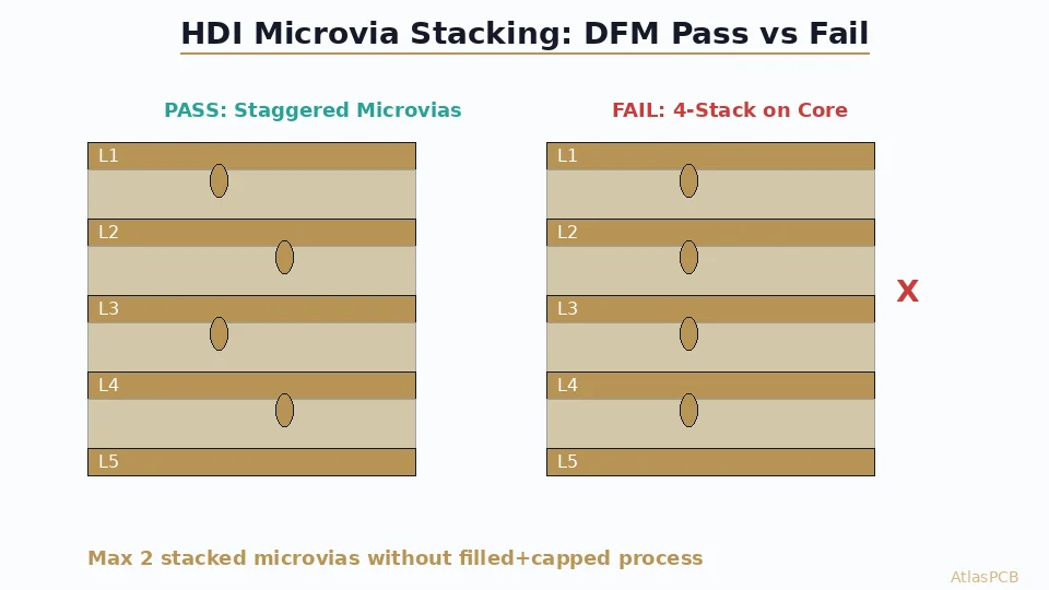
Stacked microvias—where a microvia on one layer pair is positioned directly above a microvia on the adjacent layer pair—create a continuous copper column through multiple layers. This structure provides excellent electrical performance but imposes specific fill requirements. The lower microvia must be copper-filled and planarized flat before the upper microvia is drilled into it. Any resin fill, void, or dimple in the lower via compromises the upper via’s reliability because the laser drilling and subsequent plating encounter an irregular substrate.
For designs requiring stacked microvias, our capability supports two levels of stacking reliably—meaning a via from Layer 1 to 2 stacked on a via from Layer 2 to 3, creating connectivity from Layer 1 to Layer 3 through two stacked microvias. Three levels of stacking (connecting four layers through three stacked microvias) is achievable but requires process validation for each specific design due to the cumulative effect of plating variations and thermal stress concentration at the central via.
Staggered microvias—where the upper via is offset horizontally from the lower via—relax the fill requirement because the upper via drills into solid copper of the intermediate layer pad rather than into a filled via. This configuration is inherently more reliable and manufacturable than stacked vias because each microvia acts as an independent structure. The offset distance must be at least equal to the via diameter plus registration tolerances, typically 200 micrometers minimum center-to-center between staggered vias.
Microvias landing on buried vias require the buried via to be filled and planarized before the HDI buildup layers are added. An unfilled buried via beneath a microvia target pad creates a void directly under the laser drilling target, resulting in the laser punching through into empty space rather than stopping on solid copper. Every buried via that will receive a microvia landing must be specified as filled in the fabrication documentation.
Dielectric Thickness Considerations
The dielectric thickness between layers in HDI stackups serves dual purposes: it provides impedance control for controlled-impedance routing, and it determines the achievable microvia aspect ratio. These two requirements sometimes conflict, requiring careful stackup optimization.
Standard HDI dielectric thicknesses range from 50 to 100 micrometers for the buildup layers where microvias are drilled. At 65 micrometers—the most common thickness for standard HDI—a 100 micrometer drill easily satisfies the 1:1 aspect ratio requirement. However, if impedance targets require thicker dielectric (for instance, 100 micrometers for a specific impedance on a particular trace width), the minimum via diameter must increase proportionally.
Prepreg resin content affects via filling during lamination. Higher resin content prepregs flow better during pressing, filling open vias and compensating for surface irregularities. When the design includes many buried or open vias, specifying prepreg with resin content above 60 percent helps ensure complete void-free filling. Conversely, low-resin prepregs may leave voids in via barrels that manifest as delamination during thermal excursions.
Registration and Tolerance Stack-Up
HDI fabrication involves multiple sequential processes—core drilling, inner layer imaging, lamination, laser drilling, outer layer imaging—each contributing its own position tolerance. The cumulative effect of these tolerances determines whether the designed pad sizes provide sufficient annular ring in the finished product.
For a typical 1+N+1 HDI board, the registration stack-up between a laser microvia and its target pad includes: laser-to-artwork alignment (plus or minus 25 micrometers), artwork-to-core layer shift during lamination (plus or minus 25 micrometers), and the combined effect creates a worst-case misregistration of approximately 50 micrometers. This is why our minimum target pad extends 50 micrometers beyond the drill diameter on each side—to guarantee copper contact even under worst-case conditions.
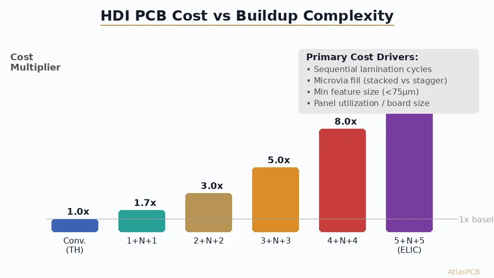
Higher-order HDI structures with multiple sequential lamination cycles accumulate additional tolerance from each lamination step. A 3+N+3 stackup undergoes three lamination cycles, each contributing 25 micrometers of potential layer shift. The cumulative tolerance demands larger pads on deeper layers, which partially offsets the routing density gain from using blind vias. Experienced HDI designers account for this by using larger pads on inner target layers while maintaining minimum pads on outer capture layers where registration is controlled by the final imaging step.
Design for Reliability: Thermal Cycling Considerations
The long-term reliability of blind and buried via structures depends on their ability to withstand the cyclic thermal expansion stresses that occur during both assembly reflow and field operation. The coefficient of thermal expansion mismatch between copper via barrels and surrounding dielectric creates strain that accumulates with each thermal cycle, eventually initiating cracks at stress concentration points.
For unfilled microvias, the weakest point is the junction between the via barrel wall and the target pad at the bottom. This corner experiences the highest stress concentration during thermal cycling as the dielectric expands vertically while the copper tries to restrain it. Adequate copper thickness in the via barrel—minimum 18 micrometers for standard reliability, 25 micrometers for high-reliability applications—provides the mechanical strength to resist crack initiation at this critical joint.
Copper-filled microvias distribute thermal stress more uniformly because the solid copper fill restrains the dielectric expansion from within the via, eliminating the barrel-to-pad stress concentration. This is why stacked microvia configurations mandate copper filling—without it, the stacked structure concentrates stress at each via-to-via interface, leading to rapid fatigue failure under thermal cycling.
Our standard reliability qualification for HDI products includes 1000 cycles of thermal cycling between minus 55 and plus 125 degrees Celsius per IPC-TM-650 2.6.7.2, with acceptance criteria requiring no resistance increase exceeding 10 percent. Designs that follow the rules outlined in this guide consistently pass this qualification without degradation.
Common DFM Violations and How to Fix Them
Having reviewed thousands of HDI designs for manufacturing feasibility, our DFM engineers encounter recurring violations that delay production starts. Understanding these common issues helps designers submit manufacturable files on the first submission.
The most frequent violation is insufficient annular ring on microvia target pads. Designers often size target pads to match the surrounding thermal relief pattern or ground plane clearance rather than the via landing requirement. The fix is simple: ensure every microvia target pad meets the minimum diameter regardless of surrounding geometry. If necessary, add an anti-pad clearance around the enlarged target pad to maintain impedance control.
Stacked vias specified without copper fill represent the second most common rejection. Designers who stack microvias without noting the fill requirement in their fabrication notes create a structure that appears geometrically valid in the CAD tool but cannot be reliably manufactured. Every stacked via must be explicitly called out as copper-filled in the fabrication drawing, with the stack direction (bottom-up or top-down) clearly specified.
Via-in-pad configurations where a blind via lands in an SMT pad without planarization specification cause assembly defects. The dimple or bump at an unfilled or poorly planarized via-in-pad creates solder voiding during reflow. For any blind via located within an SMT pad footprint, the fabrication specification must require copper filling followed by surface planarization to within plus or minus 10 micrometers of the surrounding copper surface.
Aspect ratio violations on skip vias represent a geometric error that CAD tools typically do not flag. A designer may correctly specify a microvia from Layer 1 to Layer 3, not realizing that the combined dielectric thickness of two layers exceeds the drill diameter. CAD design rule checks should be configured to verify the aspect ratio for each via span, comparing the sum of dielectric thicknesses to the drill diameter.
Specifying Your Design: Fabrication Documentation Requirements
Clear fabrication documentation prevents misinterpretation and ensures your design intent is accurately translated to the manufacturing floor. For HDI boards with blind and buried vias, the fabrication drawing must include several elements beyond standard multilayer specifications.
The stackup drawing must clearly indicate which layers are cores and which are buildup layers, with dielectric thicknesses, copper weights, and material types for each layer. Via types must be identified by layer span using the convention “L1-L2” for a via connecting Layer 1 to Layer 2, with drill diameter and pad sizes specified for each via type.
Via fill requirements must be explicitly stated. Indicate whether each via type is to be filled with copper, filled with resin, or left open. For copper-filled vias, specify the planarization tolerance. For resin-filled vias, specify whether a copper cap is required.
Sequential lamination requirements should note the number of lamination cycles and the processing sequence. This information helps the fabricator plan their production flow and verify that the design is compatible with their equipment capabilities.
Working Within Your Fabricator’s Capabilities
Not all PCB fabricators possess equal HDI capabilities. The equipment, chemistry, and process experience required for reliable HDI production represent significant capital and knowledge investments that vary across the supply chain. Before finalizing an HDI design, confirm your fabricator’s capabilities against your design requirements.
Key questions include the maximum number of sequential lamination cycles supported, minimum laser drill diameter in production (not laboratory demonstration), stacking capability (number of stacked via levels), fill type available (copper, resin, or both), and minimum dielectric thickness for reliable laser drilling. At AtlasPCB, we provide a detailed capability matrix to designers during the quotation phase, enabling informed design decisions that align with proven manufacturing capability rather than theoretical limits.
Designing to the center of your fabricator’s process window rather than the edge dramatically improves yield and reliability. A design that uses 100 micrometer microvias when 75 micrometers would suffice gains no functional advantage but sacrifices manufacturing margin that translates directly to higher yields, lower cost, and better long-term reliability.
Conclusion
Blind and buried via design for HDI PCBs requires balancing routing density requirements against manufacturing constraints that are fundamentally physical in nature. The rules presented here represent proven production capability verified through years of HDI fabrication and thousands of reliability test vehicles. Designs that respect these rules proceed smoothly through fabrication with high yields and pass stringent reliability qualification. Designs that push beyond these limits encounter DFM rejections, yield issues, or—in the worst case—field reliability concerns that trace back to manufacturing stress at via structures.
The most successful HDI designs emerge from early collaboration between the PCB designer and fabrication partner, where capability limits are understood before layout begins rather than discovered after Gerber submission. We encourage designers working on their first HDI project to engage our engineering team during the stackup definition phase, where small adjustments to layer count, dielectric thickness, or via architecture can dramatically improve manufacturability without compromising electrical performance.
Reviewed by AtlasPCB Engineering Team
Planning an HDI Design with Blind and Buried Vias?
Submit your stackup concept for a free DFM review. Our HDI engineering team will verify manufacturability and suggest optimizations before you commit to layout.
Get a QuoteAbout AtlasPCB — We specialize in complex PCB manufacturing for HDI, RF, and high-reliability applications. Explore our HDI PCB manufacturing capabilities, or get an free engineering DFM review . Every order includes free engineering review. Get your quote.
Reviewed by AtlasPCB Engineering Team — IPC-certified manufacturing specialists with 15+ years of production experience in HDI, RF, and high-reliability PCB fabrication. Content based on factory floor data and real customer design reviews.
- blind via
- buried via
- HDI PCB
- design rules
- DFM
- microvia
- PCB fabrication
- sequential lamination