· AtlasPCB Engineering · News · 7 min read
IPC-6012 Revision ES Update: Tighter Via Fill and Plating Requirements Set to Reshape HDI Manufacturing
The upcoming IPC-6012 Revision ES introduces significantly tighter requirements for via fill quality, copper plating uniformity, and hole wall integrity. Here's what PCB engineers and manufacturers need to know about the changes and their impact on HDI and high-reliability board production.
IPC-6012 Revision ES Update: Tighter Via Fill and Plating Requirements Set to Reshape HDI Manufacturing
The IPC is preparing to release the most significant update to its flagship rigid PCB qualification standard in over five years, and the changes will have real-world consequences for every fabricator producing HDI and high-reliability printed circuit boards.
IPC-6012 Revision ES — currently in draft review with final ballot expected in Q3 2026 — introduces substantially tighter requirements for via fill quality, copper plating uniformity, and hole wall integrity. These aren’t cosmetic changes: they reflect the evolving demands of advanced electronics where via structures serve as critical signal and thermal pathways, not just simple layer-to-layer connections.
Why Via Fill and Plating Standards Need Updating
The current IPC-6012 revision (DS, published in 2023) was developed when the most demanding mainstream PCB designs featured 12–16 layers with mechanical drill vias and standard copper plating. The landscape has shifted:
- HDI designs with stacked microvias, via-in-pad, and sequential lamination are now standard for smartphones, AI hardware, automotive radar modules, and medical devices
- Via-in-pad with filled and capped vias is required for fine-pitch BGA components (0.5mm pitch and below), where any via dimple can cause solder joint reliability issues
- Thermal via arrays under power components and LED arrays must conduct heat efficiently, making void-free fill a functional requirement rather than merely cosmetic
- High-speed designs use back-drilled vias where consistent plating thickness affects the remaining stub length and, consequently, signal integrity at 56+ Gbps
The existing acceptance criteria, written for a previous generation of PCB complexity, have become insufficient for today’s designs.
Key Changes in Revision ES
The draft introduces changes across several critical areas:
1. Via Fill Void Requirements
Current standard (DS): Class 3 boards allow up to 25% void area in filled vias when measured by cross-section analysis.
Revision ES: Class 3 void limit reduced to 10%. A new Class 3/A designation for aerospace and defense applications limits voids to 5% and requires 100% X-ray inspection of filled vias on qualification lots.
This is the single most impactful change for manufacturers. Achieving consistent sub-10% void fill requires precise control of fill material viscosity, screen printing parameters, and vacuum-assisted filling processes. Many fabricators currently operate at 15–20% void levels for Class 3 work — they will need to upgrade processes.
2. Dimple Depth Limits
Current standard: No explicit dimple depth limit; assessed subjectively as “acceptable” or “not acceptable” with reference images.
Revision ES: Maximum dimple depth of 75μm for Class 3, 50μm for Class 3/A. Dimple depth is measured from the surrounding copper surface to the lowest point of the depression after cap plating.
This change directly affects [via fill and cap plating processes]/blog/pcb-blind-via-fill-technology/). Fabricators using non-optimized fill materials or inadequate planarization grinding will need to improve their processes to meet these tighter limits consistently.
3. Copper Plating Uniformity
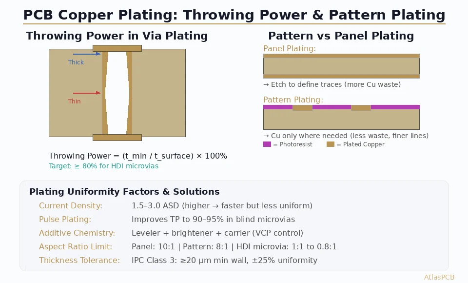
Current standard: Plating thickness uniformity of ±25% across the panel for Class 3.
Revision ES: Tightened to ±15% for Class 3, with an additional requirement that minimum plating thickness in any via hole must not fall below 20μm (previously 18μm).
The uniformity requirement is particularly challenging for panels with mixed feature sizes — a common scenario in HDI designs where 0.1mm laser-drilled microvias coexist with 0.3mm mechanical drills on the same layer. Achieving uniform plating across these different feature sizes requires advanced pulse plating or reverse-pulse plating equipment and carefully optimized bath chemistry.
4. Via Fill Material Thermal Stability
New requirement in ES: Via fill material must demonstrate:
- Adhesion retention after 6x reflow simulation at 260°C peak temperature
- Fill material shrinkage not exceeding 15μm after thermal stress testing at 288°C for 10 seconds
- No delamination, cracking, or separation visible at 200x magnification after thermal cycling (–55°C to +125°C, 1000 cycles)
This addresses a known field reliability issue where some via fill materials shrink or separate from the barrel wall after repeated thermal cycling, creating intermittent open circuits that are extremely difficult to diagnose. The new requirements will force material qualification testing that many fill material suppliers have not previously been required to provide.
5. Hole Wall Quality for Back-Drilled Vias
New requirement in ES: For back-drilled vias, the remaining stub length must be controlled to within ±50μm of the design target (previously no explicit tolerance was defined). Additionally, the drill re-entry point must show no more than 25μm of copper pullback from the barrel wall.
This reflects the growing importance of [via reliability]/blog/pcb-via-reliability-testing/) in high-speed designs where back-drill accuracy directly impacts signal integrity performance.
Impact on Manufacturers and the Supply Chain
The tightened requirements will create a clear capability divide in the fabrication market:
Tier 1 manufacturers with modern equipment (vacuum-assisted via fill, advanced pulse plating, automated cross-section analysis) will likely meet the new requirements with process adjustments rather than capital investment.
Mid-tier fabricators — the majority of the market — will face a choice: invest in equipment upgrades (estimated $2–5 million per line for via fill and plating improvements) or concede the Class 3/A and advanced HDI market segments.
Material suppliers will need to provide more comprehensive qualification data for via fill materials, including thermal cycling performance and shrinkage data that many currently don’t include in their datasheets.
For engineers specifying [IPC Class 3 requirements]/blog/ipc-class-3-requirements/), the revision means more confidence that “Class 3” actually delivers the reliability implied by the designation — but it also means ensuring your chosen fabricator can meet the new standard.
What Engineers Should Do Now
Review your via fill specifications: If you’re currently calling out “IPC-6012 Class 3” on your fabrication notes, understand that the requirements are about to get significantly tighter. Discuss with your fabricator whether they can meet Revision ES requirements today.
Design with fill quality in mind: Aspect ratios matter. A 0.1mm via in a 1.0mm-thick board (10:1 aspect ratio) is far more challenging to fill void-free than a 0.2mm via in the same board. Where possible, optimize via sizes to improve fill quality.
Specify fill material properties: For high-reliability applications, consider specifying via fill materials by name or by performance properties (CTE, Tg, thermal conductivity) rather than leaving the choice entirely to the fabricator.
Request cross-section data: Ask your fabricator to provide cross-section photographs of via fill quality from recent production lots. This establishes a baseline and opens a dialogue about their capability relative to the new standard.
Timeline and Adoption
The expected timeline for IPC-6012 Revision ES:
- Q2 2026: Final draft review and comment resolution
- Q3 2026: Industry ballot
- Q4 2026 – Q1 2027: Publication
- 2027–2028: Gradual adoption into OEM procurement specifications
Major defense and aerospace OEMs are expected to reference Revision ES within 6 months of publication. Commercial electronics OEMs will likely follow within 12–18 months. This gives manufacturers a window to prepare — but that window is shorter than it appears, given the capital investment timelines involved.
The message is clear: the bar for PCB via fill and plating quality is being raised. Manufacturers and engineers who prepare now will be ready when the new standard becomes the baseline expectation for high-reliability electronics.
AtlasPCB Engineering maintains active participation in IPC standards development and ensures manufacturing processes align with the latest requirements. For questions about IPC-6012 compliance or HDI capabilities, contact us.
About AtlasPCB — We specialize in complex PCB manufacturing for HDI, RF, and high-reliability applications. Explore our HDI PCB manufacturing capabilities, or get an full PCB manufacturing capabilities . Every order includes free engineering review. Get your quote.
Reviewed by AtlasPCB Engineering Team — IPC-certified manufacturing specialists with 15+ years of production experience in HDI, RF, and high-reliability PCB fabrication. Content based on factory floor data and real customer design reviews.
- industry-news
- ipc-standards
- via-fill
- plating
- hdi-pcb