· AtlasPCB Engineering · News · 4 min read
SMTA Capital Expo 2026: X-Ray and CT Inspection Take Center Stage as PCB Complexity Drives Demand for Non-Destructive Analysis
At SMTA Capital Expo in Baltimore, TTCI showcases X-ray and CT inspection capabilities alongside traditional electrical test, highlighting the growing need for non-destructive internal analysis as PCB assemblies grow denser and more complex.
X-Ray and CT Inspection Move from Lab Curiosity to Production Necessity
May 10, 2026 — As PCB assemblies grow denser, components shrink, and reliability expectations climb, the electronics manufacturing industry is increasingly turning to X-ray and computed tomography (CT) inspection as essential tools—not just for failure analysis, but as integrated steps in production workflows.
This shift was on full display at the announcement that The Training Connection LLC (TTCI) will showcase its expanded inspection capabilities at the SMTA Capital Expo on May 14 in Baltimore, as reported by SMT Today.
Beyond Electrical Test: Why X-Ray Matters
TTCI, known primarily for over 45 years of electrical test services (ICT, flying probe, boundary scan, and functional test), is highlighting its Prime TruVision™ X-ray and CT Inspection System from Creative Electron. The system supports three distinct imaging modes:
- 2D X-ray: Rapid inspection of solder joints, component placement, and internal layer alignment
- Laminography: Angled X-ray imaging that provides depth-selective views of specific layers within a dense assembly
- Full 3D CT scanning: Complete volumetric reconstruction enabling inspection of internal structures from any angle
This multi-modal approach enables engineers to examine internal structures in high detail without destructive analysis—a critical capability when investigating issues that electrical test alone cannot explain.
Use Cases Driving Adoption
The technology is particularly valuable for inspecting:
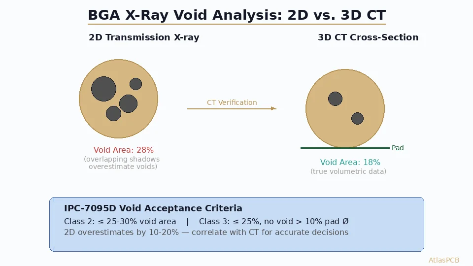
- BGA and QFN solder joints: Hidden solder connections beneath components where visual inspection is impossible. X-ray reveals voiding percentages, bridging, and incomplete wetting
- Via integrity: Examining plated through holes, buried vias, and microvias for barrel cracks, plating voids, and delamination
- Component-level defects: Identifying internal die fractures, wire bond failures, or package-level anomalies
- Counterfeit detection: Comparing internal die structures against known-good reference samples
Integration with Electrical Test Workflows
Rather than treating inspection and electrical test as separate activities, the industry is moving toward integrated engineering workflows. As TTCI describes it: electrical test confirms whether the assembly performs to specification, while X-ray and CT help pinpoint the root cause when something isn’t right.
This integrated approach delivers faster resolution. Instead of a failed ICT test triggering a separate failure analysis request—which might take days or weeks—the same service provider can immediately image the suspect area and identify whether the issue is a solder void, a cracked via barrel, or a component-level defect.
Industry Context: Why Now
Several converging trends are accelerating X-ray and CT adoption in PCB manufacturing:
Miniaturization: As component packages shrink (0201, 01005 passives, 0.3mm pitch BGAs), there are simply fewer visible solder joints to inspect optically. Traditional AOI systems reach their limits when connections are hidden beneath package bodies.
HDI complexity: With [stacked and staggered microvias]/blog/hdi-microvia-stacked-vs-staggered-reliability/), buried vias, and increasingly complex layer stackups, the internal structure of modern PCBs is far more intricate than legacy designs. Verifying via fill quality and interlayer connections requires volumetric imaging.
Reliability demands: Industries like aerospace, medical, and automotive require Class 3 [IPC standards compliance]/blog/ipc-a-600-class-2-vs-class-3-pcb-acceptability/) with documented evidence that internal structures meet specification. X-ray provides objective, archivable evidence.
Cost of failure: As boards become more expensive (high-layer HDI boards can cost $500-2000+ per unit), the economics favor investing in thorough inspection over scrapping expensive assemblies.
The Broader SMTA Capital Expo Context
The SMTA Capital Expo, held annually in the Baltimore–Washington corridor, brings together electronics manufacturing professionals from defense, aerospace, and government-adjacent sectors—industries where inspection rigor is non-negotiable. Other exhibitors at this year’s event include thermal process control specialists and cleaning chemistry providers, reflecting the industry’s growing focus on process monitoring and quality assurance throughout the entire assembly workflow.
What This Means for PCB Design Engineers
Design engineers should consider inspection requirements early in the design process:
- Design for Inspection (DFI): Provide X-ray access paths in your BGA placement. Avoid stacking large BGAs directly above each other on opposite sides—this creates overlapping X-ray shadows
- Via inspection requirements: If your design uses [via-in-pad with plated over]/blog/pcb-via-in-pad-plated-over-design/), specify voiding acceptance criteria in your fabrication notes
- Document acceptance criteria: Include specific X-ray voiding limits (typically ≤25% for Class 2, ≤10% for Class 3) in your assembly specifications
At AtlasPCB, our PCBA assembly services include X-ray inspection as a standard quality gate for BGA and hidden-joint assemblies. We can also provide CT scan reports for critical reliability applications. Contact us to discuss inspection requirements for your next project.
Source: SMT Today, iConnect007
Image: ThisisEngineering via Unsplash
About AtlasPCB — We specialize in complex PCB manufacturing for HDI, RF, and high-reliability applications. Explore our HDI PCB manufacturing capabilities, PCB assembly services, or get an full PCB manufacturing capabilities . Every order includes free engineering review. Get your quote.
Reviewed by AtlasPCB Engineering Team — IPC-certified manufacturing specialists with 15+ years of production experience in HDI, RF, and high-reliability PCB fabrication. Content based on factory floor data and real customer design reviews.
- news
- X-ray inspection
- CT scanning
- SMTA
- PCB testing
- non-destructive testing
- BGA inspection
- quality control
- electronics manufacturing