· AtlasPCB Engineering · News · 4 min read
PCB Forge: New Open-Source Tool Enables 3D-Printed Circuit Boards
A new open-source tool called PCB Forge lets makers create functional PCBs using 3D printers and copper tape — no chemicals required. Here's what it means for prototyping.
A Clever New Approach to Rapid PCB Prototyping
The PCB prototyping landscape gained a creative new tool in early 2026: PCB Forge, an open-source web application that converts SVG circuit designs into 3D-printable molds for creating functional printed circuit boards without any chemical etching. Reported by Hackaday in February 2026, the tool has generated significant interest in the maker and engineering prototyping communities.
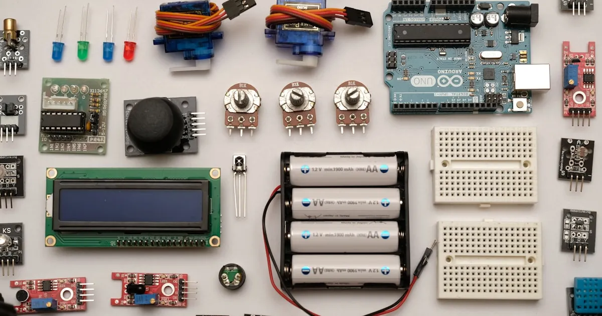
Photo by ThisisEngineering on Unsplash — Free to use under Unsplash License
How PCB Forge Works
The workflow is elegantly simple:
- Design your traces in any vector editor (Inkscape, Adobe Illustrator, or even export from KiCad/Eagle)
- Export as SVG with your circuit traces as paths
- Upload to PCB Forge — the web tool automatically generates two 3D-printable parts: a base and a companion mold
- 3D print both parts on any standard FDM printer
- Apply copper tape (with conductive adhesive) across the entire surface of the base part
- Press the companion mold onto the base — this pushes copper tape into all the recessed trace channels
- Remove the mold and sand — carefully sand off the exposed copper between traces
- Solder your components directly to the copper tape traces
The tool automatically calculates correct clearances and generates alignment features, making the press-together step reliable and repeatable. The entire process from SVG to soldering-ready board can be completed in under an hour, depending on 3D print time.
What It Can (and Can’t) Do
Strengths
- No chemicals: Eliminates the need for ferric chloride, ammonium persulfate, or other etchants — making it ideal for environments where chemical handling isn’t practical (classrooms, home workshops, hackathons)
- No special equipment: Requires only a standard 3D printer and copper tape, both widely available
- Rapid iteration: Print a new mold for each design revision — no waiting for board houses or chemical preparation
- Educational value: The physical process of pressing copper into trace shapes provides intuitive understanding of how PCB traces work
Limitations
This technique is fundamentally limited to simple, single-layer designs. It’s important to understand what professional [PCB manufacturing]/blog/pcb-manufacturing-process/) provides that 3D-printed PCBs cannot:
| Feature | 3D-Printed PCB | Professional PCB |
|---|---|---|
| Layer count | 1 (single-sided) | 1–68+ layers |
| Trace width | ~1mm minimum | 3 mil (75μm) minimum |
| Via support | None | Through, blind, buried, microvias |
| Impedance control | Not possible | ±10% per [IPC standards]/blog/pcb-impedance-control/) |
| Plating | Copper tape adhesive | 25μm+ electroplated copper |
| Surface finish | None | ENIG, HASL, OSP, etc. |
| Solder mask | None | Standard |
| Reliability | Hobby grade | [IPC-6012 Class 2/3]/blog/ipc-standards-pcb-classes/) |
The creator, [castpixel], built PCB Forge as an expansion of techniques demonstrated by [QZW Labs], who showed that copper tape on 3D-printed substrates could create functional circuits. PCB Forge makes the process more accessible by automating the 3D model generation.
When DIY Prototyping Makes Sense
Tools like PCB Forge fill a genuine gap in the prototyping workflow. There are scenarios where waiting even 24–48 hours for a prototype board isn’t acceptable:
- Concept validation: Testing whether a basic circuit topology works before investing in a proper PCB design
- Hackathon projects: Building functional hardware in 24–48 hours where speed trumps all other considerations
- Education: Teaching PCB concepts in classrooms where chemical handling isn’t permitted
- Art and creative electronics: LED installations, interactive sculptures, and wearable projects where traces are visible design elements
However, once a design moves beyond concept validation — when you need controlled impedance, multiple layers, reliable solder joints, or any kind of volume production — professional fabrication becomes essential. The gap between a copper-tape prototype and a professionally manufactured board isn’t just about aesthetics; it’s about electrical performance, mechanical reliability, and long-term durability.
The Broader Trend: PCB Fabrication Accessibility
PCB Forge is part of a broader trend toward making PCB creation more accessible to hobbyists and small teams. The PCB fabrication industry itself has already undergone remarkable democratization over the past decade:
- Online ordering: Upload Gerbers, get boards in days
- Price compression: Simple 2-layer boards for under $5 in small quantities
- Rapid prototyping services: 24-hour turn times from multiple fabricators
- Open-source EDA: KiCad, FreeRouting, and other tools eliminate software costs
At the same time, board houses are competing for the enthusiast market with innovations like transparent flexible PCBs, glow-in-the-dark substrates, and diverse solder mask color options — features that were unimaginable in the professional-only PCB world of even a decade ago.
Atlas PCB: When You’re Ready for Production Quality
While we appreciate and encourage the maker community’s creativity with tools like PCB Forge, there comes a point in every project where professional fabrication is the right choice. Atlas PCB offers 24-hour prototype turnaround for designs that need:
- Multi-layer stackups with [impedance control]/blog/pcb-impedance-control/)
- Fine-pitch BGA routing with [HDI technology]/blog/hdi-pcb-technology/)
- Controlled surface finishes per [IPC-6012]/blog/pcb-surface-finish-guide/)
- Volume production with consistent quality
Ready to move from prototype to production? Upload your Gerbers for an instant quote with free DFM review, or contact our engineering team to discuss your project requirements.
About AtlasPCB — We specialize in complex PCB manufacturing for HDI, RF, and high-reliability applications. Explore our full PCB manufacturing capabilities, or get an instant online quote . Every order includes free engineering review. Get your quote.
Reviewed by AtlasPCB Engineering Team — IPC-certified manufacturing specialists with 15+ years of production experience in HDI, RF, and high-reliability PCB fabrication. Content based on factory floor data and real customer design reviews.
- news
- pcb-prototyping
- 3d-printing
- open-source
- maker