· AtlasPCB Engineering · News · 4 min read
Intel Rio Rancho Targets World's First Mass Production of Glass Substrates for AI Chip Packaging
Intel Foundry's New Mexico facility moves toward becoming the first factory to mass-produce glass substrates, a critical technology for next-generation AI chip packaging. AWS, Cisco, and reportedly Apple, Google, Nvidia, and Tesla are engaging with the platform.

Intel Foundry Positions Rio Rancho for Glass Substrate Volume Production
Reports from Wccftech and Forbes on May 26, 2026, indicate that Intel Foundry’s facility in Rio Rancho, New Mexico, is advancing toward becoming the world’s first factory to achieve mass production of glass substrates — a next-generation chip packaging technology considered critical for scaling AI hardware beyond current organic substrate limitations.
The facility, which has already begun manufacturing silicon photonics products for external customers, is expected to play a central role in Intel’s advanced packaging strategy. While Intel’s Chandler, Arizona site currently operates glass substrate pilot lines, Rio Rancho is reportedly targeting full-scale production capabilities.
Why Glass Substrates for AI
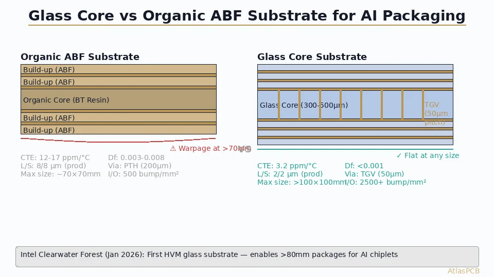
Glass substrates address fundamental limitations of current organic (ABF) substrates that are becoming bottlenecks for AI chip scaling:
Critical advantages for AI packaging:
- Extreme flatness (<1 μm warpage) enables larger die and chiplet assemblies
- Low CTE (3-8 ppm/°C) closely matches silicon (2.6 ppm/°C), reducing thermal stress in multi-chip packages
- Higher interconnect density: Finer features possible due to dimensional stability
- Better high-frequency performance: Low dielectric loss for high-speed I/O
- Larger format: Can support bigger interposers than organic substrates
For AI accelerators that already push the limits of organic CoWoS substrates at 5,500+ mm², glass substrates could enable even larger multi-chiplet assemblies without the warpage and registration challenges that plague oversized organic packages.
Intel’s Advanced Packaging Ecosystem
Intel has been building an advanced packaging portfolio that complements glass substrate technology:
Current Technologies
- EMIB (Embedded Multi-die Interconnect Bridge): Enables high-density die-to-die connections on organic substrates
- Foveros: 3D stacking technology for logic-on-logic packaging
- Co-Packaged Optics (CPO): Intel recently showcased glass-core substrate prototypes integrated with CPO
Customer Base
According to the Forbes report, Intel Foundry’s advanced packaging customers and discussions include:
- Existing customers: Amazon Web Services (AWS), Cisco
- Reportedly in discussion: Apple, Google, Microsoft, Nvidia, Tesla
This customer list spans the complete AI hardware spectrum — from hyperscaler custom silicon (AWS, Google, Microsoft) to autonomous driving (Tesla) to general-purpose AI acceleration (Nvidia).
Commercial Timeline and Competitive Landscape
Intel first introduced glass substrate technology publicly in 2023. The current roadmap:
| Milestone | Timeline |
|---|---|
| Glass substrate R&D announcement | 2023 |
| Pilot line (Chandler, AZ) | 2024-2025 |
| Silicon photonics production (Rio Rancho) | 2026 (active) |
| Glass substrate volume production | ~2028-2030 |
| Full commercial deployment | ~2030 |
Global Competition
The race for glass substrate commercialization is intensifying:
- SKC/Absolics (Korea): Operating pilot lines, targeting 2027 commercial supply
- Samsung Electro-Mechanics (Korea): Advancing pilot production
- Chinese consortium (GCPA): Just formed industry alliance to accelerate domestic development
- YCChem (Korea): Recently started commercial supply of glass substrate photoresist materials
Intel’s advantage lies in its integrated approach — controlling both the substrate manufacturing and the advanced packaging (EMIB, Foveros) that uses them. This vertical integration allows co-optimization that standalone substrate manufacturers cannot achieve.
Implications for the PCB and Substrate Industry
Near-Term (2026-2028)
- Glass substrates remain in pilot/limited production
- Organic ABF substrates continue as the primary platform
- PCB motherboards and backplanes unchanged by glass substrate development
- Testing and characterization boards needed for glass substrate qualification
Medium-Term (2028-2032)
- Glass substrates enter volume for premium AI packages
- Organic substrates remain dominant for non-AI applications
- PCB-to-glass-substrate interfaces require new assembly processes
- Board designers must account for different CTE behavior at solder joints
What PCB Manufacturers Should Prepare For
- Higher-reliability solder joints at glass-substrate-to-PCB interface
- New inspection requirements for glass-assembled modules
- Supporting test and characterization vehicles during customer qualification
- Potential changes in motherboard design rules around socket areas
Connection to AtlasPCB Capabilities
While glass substrates operate at a different tier than standard PCB manufacturing, the broader advanced packaging ecosystem creates demand for:
- Test boards: High-layer-count boards for substrate electrical characterization
- Interposer test vehicles: PCBs that mate with prototype glass substrates for validation
- AI server motherboards: The multilayer boards that glass-substrate AI processors mount to
- Signal integrity test coupons: Controlled impedance structures for validating glass-to-PCB transitions
The glass substrate revolution won’t eliminate PCBs — it will raise the performance bar for the boards that support next-generation packaged devices.
Sources: Wccftech and Forbes reports, May 26, 2026; IC&PCB Union.
Image: Laura Ockel via Unsplash
Building boards for next-generation AI hardware? AtlasPCB provides advanced multilayer PCBs with controlled impedance for AI server applications. Discuss your project →
About AtlasPCB — We specialize in complex PCB manufacturing for HDI, RF, and high-reliability applications. Explore our impedance-controlled PCB manufacturing . Every order includes free engineering review. Get your quote.
Reviewed by AtlasPCB Engineering Team — IPC-certified manufacturing specialists with 15+ years of production experience in HDI, RF, and high-reliability PCB fabrication. Content based on factory floor data and real customer design reviews.
- news
- Intel
- glass substrate
- AI packaging
- Rio Rancho
- advanced packaging
- EMIB
- Foveros
- co-packaged optics
- semiconductor
- AI