· Industry News · 6 min read
ACCM Launches Celeritas Negative-CTE PCB Material to Solve AI Chip Warpage and Signal Loss
Advanced Chip and Circuit Materials (ACCM) announces Celeritas HM50 and HM001 — purpose-built PCB laminates that eliminate warpage and high-frequency signal loss in large-format AI accelerator packages. What this means for high-layer-count board design.
What Happened
Advanced Chip and Circuit Materials (ACCM) on June 15, 2026 announced commercial availability of two new PCB laminate materials:
- Celeritas HM50: Negative CTE (-8 ppm/C) material for power plane layers
- Celeritas HM001: Near-zero CTE material with Tier 9 electrical loss performance for signal layers
Together in a single stackup, they bring board CTE below 10 ppm/C while simultaneously supporting 100+ Gbps data rates — solving two problems that previously required separate (and often conflicting) solutions.
Why This Matters for PCB Engineers
The Problem Being Solved
Every hyperscaler building AI accelerator infrastructure confronts two converging constraints:
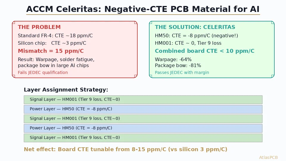
Thermomechanical warpage: Silicon CTE (2-4 ppm/C) vs standard PCB material CTE (~18 ppm/C) creates catastrophic reflow warpage in large-format packages. As AI chips scale beyond reticle limits, the mismatch literally tears solder joints apart.
Signal loss at extreme data rates: HBM, UCIe, and chip-to-chip interconnects running at 100+ Gbps push signal integrity requirements beyond what standard dielectrics can deliver.
These problems have historically been treated separately — thermal engineers optimizing CTE with one set of materials while signal integrity engineers demanded low-Dk/Df from another. The two goals often conflict.
What ACCM Claims
| Metric | Standard FR-4 | With Celeritas HM50 | Improvement |
|---|---|---|---|
| Board CTE | ~18 ppm/C | <10 ppm/C | >44% reduction |
| Warpage | Fails JEDEC qual | Passes with margin | 64% reduction |
| Package bow | Exceeds limits | Within spec | 81% reduction |
| Signal loss | Standard Tier | Tier 9 (HM001) | Best-in-class |
| Solder joint fatigue | Critical risk | >100x improvement | Major |
The key innovation: HM50 has negative CTE (-8 ppm/C), meaning it actively contracts when heated — counterbalancing the expansion of other board materials. By tuning the ratio of HM50 layers to standard layers, engineers can dial board CTE to any target between 8-15 ppm/C.
HIGH-LAYER-COUNT CAPABILITY
Building AI Accelerator Boards?
AtlasPCB fabricates boards up to 30 layers with advanced materials including high-Tg, low-loss laminates, and controlled-CTE stackups for demanding thermal environments.
Discuss Your Stackup ›How It Fits into a Stackup
ACCM proposes a layer-by-layer material assignment:
- Signal layers: Celeritas HM001 (near-zero CTE + Tier 9 loss performance)
- Power plane layers: Celeritas HM50 (negative CTE, drives board-level CTE down)
- Combined effect: Total board CTE tunable from 8-15 ppm/C depending on layer ratio
This approach means engineers do not need to pick between thermal performance and electrical performance — each layer gets the material optimized for its function.
Implications for Current AI Board Designs
For engineers currently designing 16-30 layer boards for AI inference/training cards:
- Warpage management becomes material-driven rather than mechanical (no more expensive stiffening frames or mechanical constraints during reflow)
- Signal layer loss improves without changing trace geometry or stackup height
- BGA reliability improves dramatically — reduced CTE mismatch means less solder joint fatigue over thermal cycling
vs. Glass Substrate Approach
The industry has been watching glass substrate technology (from companies like Absolics, SKC) as a potential solution to CTE mismatch. ACCM explicitly positions against glass:
| Factor | Glass Substrate | Celeritas |
|---|---|---|
| CTE | Positive (3-8 ppm/C) | Tunable (negative to zero) |
| Electrical performance | Not addressed | Tier 9 loss |
| Processing | Requires new equipment | Compatible with existing PCB processes |
| Availability | Limited pilot lines | Commercial now |
ADVANCED MATERIALS
Low-Loss Laminates for High-Speed Design
We work with Rogers, Isola, Panasonic Megtron, and other advanced laminates for demanding signal integrity applications. Talk to our materials engineering team.
View RF/High-Speed Services ›Industry Context
This announcement comes amid broader supply chain pressures in AI PCB materials:
- T-glass fiber cloth shortage constraining high-end laminate production (Digitimes, June 11)
- Lead times for advanced PCB materials stretching past 20 weeks (Digitimes, June 5)
- Nvidia driving HVLP4 copper foil demand upstream (Digitimes, June 11)
ACCM’s Celeritas entering commercial production potentially adds another high-demand material to an already-constrained supply chain. Early adopters will likely be hyperscaler programs (Google, Meta, Microsoft, Amazon) where the performance gains justify premium pricing and dedicated supply agreements.
What to Watch
- Pricing: ACCM has not disclosed material cost. Expect significant premium over standard high-speed laminates initially.
- Processing compatibility: Claim of compatibility with existing PCB processes needs validation across multiple fabs.
- Qualification data: Full JEDEC qualification data and multi-fab consistency data will determine adoption speed.
- Supply availability: A new material from a newer company always carries supply continuity risk for volume programs.
MATERIAL EXPERTISE
Need Help Selecting PCB Materials?
Whether you are evaluating new laminates for thermal performance or choosing between Rogers, Megtron, and Tachyon for signal integrity — our engineers can advise based on your specific design constraints.
Get Material Recommendation ›Practical Takeaway
For engineers designing AI accelerator boards today: Celeritas is worth evaluating if your current stackup fails JEDEC warpage qualification or if you are struggling to meet loss budgets at 56+ Gbps per lane. The material is commercially available now, but expect to work directly with ACCM for supply allocation and processing guidance during this early phase.
For most standard high-speed designs (servers, networking, telecom) below the hyperscaler tier, existing materials like Megtron 6/7 and Tachyon 100G remain proven, available, and cost-effective choices.
ATLASPCB
Advanced Material Processing Capability
From standard FR-4 to Rogers, PTFE, and high-Tg polyimide — we process the materials your design demands. Up to 30 layers with controlled impedance.
Get Instant Quote ›Related Reading:
About AtlasPCB — We specialize in complex PCB manufacturing for HDI, RF, and high-reliability applications. Explore our impedance-controlled PCB manufacturing . Every order includes free engineering review. Get your quote.
Reviewed by AtlasPCB Engineering Team — IPC-certified manufacturing specialists with 15+ years of production experience in HDI, RF, and high-reliability PCB fabrication. Content based on factory floor data and real customer design reviews.
- PCB materials
- AI accelerator
- CTE warpage
- signal integrity
- advanced packaging