· AtlasPCB Engineering · News · 5 min read
TSMC Pushes CoPoS Exclusivity to Lock In Next-Gen Packaging Lead — CoWoS Capacity to Hit 140,000 Wafers/Month by End of 2026
TSMC accelerates panel-level CoPoS packaging development with strict confidentiality controls while ramping CoWoS capacity to 115,000-140,000 wafers per month by end of 2026. The advanced packaging race intensifies as AI chip demand outstrips available capacity across the industry.

TSMC Locks Down CoPoS Supply Chain with Strict Confidentiality Controls
May 10, 2026 — TSMC is accelerating the expansion of its CoWoS advanced packaging capacity while simultaneously pushing forward with CoPoS (Chip-on-Panel-on-Substrate)—a more technically demanding panel-level packaging technology aimed at widening its lead in the AI semiconductor packaging race.
According to industry sources reported by DigiTimes, TSMC has imposed strict confidentiality controls across the entire CoPoS supply chain, requiring Taiwan-based equipment and materials partners to limit information sharing. This exclusivity approach signals that TSMC views panel-level packaging as a critical competitive moat—not just a manufacturing capability.
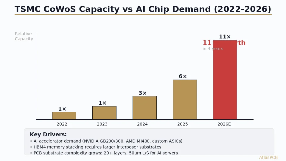
CoWoS Capacity Ramp: From 35K to 140K Wafers/Month
The numbers tell the story of explosive demand. According to institutional investors cited by TrendForce:
| Timeline | CoWoS Capacity (wafers/month) |
|---|---|
| 2024 | ~35,000 |
| End of 2026 (projected) | 115,000 – 140,000 |
| 2027 (projected) | ~170,000 |
This represents a 4× increase in just two years. Yet even at 140,000 wafers per month, demand continues to outstrip supply. NVIDIA, Google, Amazon, and MediaTek have all been reported as having their CoWoS orders fully booked, with supply-chain reports describing severe short supply for both CoWoS-L and CoWoS-S variants.
CoWoS Roadmap: 14-Reticle Packages and 48× Compute Power
At the North American Technology Symposium 2026, TSMC revealed its updated CoWoS packaging roadmap with transformative enhancements, as reported by Tom’s Hardware:
- Package size: Scaling to over 14 reticle sizes—enabling enormous interposer areas that can accommodate multiple chiplets plus extensive HBM stacks
- HBM integration: Support for up to 24 HBM5E stacks on a single package
- Compute density: A projected 48× leap in compute power by 2029 compared to current generation
- Memory bandwidth: Substantial bandwidth improvements from the sheer number of HBM stacks
The message is clear: packaging is now the scaling engine. As transistor-level scaling slows, the ability to integrate more dies, more memory, and more I/O within a single package becomes the primary differentiator for AI compute performance.
What CoPoS Means for the PCB Substrate Ecosystem
CoPoS (panel-level packaging) represents a fundamental shift in how advanced packages are manufactured. Instead of processing individual wafers, CoPoS works with larger rectangular panels—similar to how PCBs are manufactured. This offers several advantages:
- Higher throughput: Larger panel area means more packages per processing cycle
- Lower cost per unit: Panel-level processing amortizes equipment costs over more units
- Larger package sizes: Panel format enables package sizes that are impractical on round wafers
For the PCB and substrate industry, this convergence is significant. As reported in our earlier coverage of [IC substrates vs HDI PCBs]/blog/ic-substrate-vs-hdi-pcb-substrate-like-pcb-slp-technology/), the boundary between semiconductor packaging and PCB fabrication continues to blur. Panel-level packaging uses many of the same materials and processes as advanced PCB manufacturing—copper redistribution layers, build-up dielectrics, and fine-line patterning.
Implications for Hardware Engineers
The advanced packaging capacity crunch has cascading effects:
- Lead times: AI-class designs requiring CoWoS packaging face 6-12 month lead times for packaging slots
- Substrate demand: The ramp in advanced packaging is consuming high-end ABF substrates and [HDI PCB]/blog/hdi-pcb-stackup-design-advanced/) materials at unprecedented rates, contributing to the broader [CCL shortage]/news/news-ccl-market-korea-import-prices-surge-74-percent-ai-demand-2026/)
- Design implications: Engineers designing systems that interface with CoWoS-packaged devices need to account for increasingly complex BGA patterns, tighter ball pitch, and higher pin counts on their host PCBs
- Alternative approaches: For designs where CoWoS lead times are prohibitive, [multi-chip module approaches using advanced HDI PCBs]/blog/hdi-pcb-stackup-design-advanced/) can provide a faster path to market
The Broader Advanced Packaging Landscape
TSMC is not alone in the advanced packaging race. The competitive landscape is intensifying:
Intel (EMIB + Foveros): Intel’s Embedded Multi-Die Interconnect Bridge (EMIB) technology competes directly with CoWoS for heterogeneous die integration. Intel has committed to expanding its advanced packaging capacity in New Mexico and Malaysia, though it remains significantly behind TSMC in production volume.
Samsung (I-Cube): Samsung’s I-Cube 2.5D packaging technology is ramping for HBM integration, primarily serving its own foundry customers. Samsung has announced plans to double its advanced packaging capacity by 2027.
OSAT Players: Traditional outsourced semiconductor assembly and test companies (ASE, Amkor, JCET) are investing in fan-out wafer-level packaging and panel-level packaging alternatives. As covered in our earlier reporting, [ASE, Samsung, and Amkor announced $15B+ in new facilities]/news/news-ase-samsung-amkor-packaging-capacity-expansion-2026/) for 2026-2027.
Supply Chain Ripple Effects
The advanced packaging capacity crunch creates cascading effects across the electronics supply chain:
ABF substrate demand: CoWoS and competing technologies consume enormous quantities of ABF (Ajinomoto Build-up Film) substrates. The [ABF substrate market has hit $7.19 billion]/news/news-abf-substrate-market-7-billion-advanced-packaging-2026/), with suppliers like Ibiden, Shinko, and Unimicron operating at near-full utilization. This directly competes with advanced PCB production for high-end materials.
HBM production: Each CoWoS package integrates multiple HBM (High Bandwidth Memory) stacks. SK Hynix and Samsung are ramping HBM3E and early HBM4 production, but the supply of tested-good HBM stacks constrains how many complete packages TSMC can deliver—even if packaging capacity were unlimited.
PCB-level impact: System boards that host CoWoS-packaged processors must accommodate increasingly complex ball grid arrays—sometimes exceeding 5,000 pins at fine pitch. This drives demand for high-layer-count PCBs with [controlled impedance]/blog/controlled-impedance-pcb-design-stackup-calculations/) and tight BGA routing—exactly the type of boards that require premium CCL grades currently in shortage.
Looking Ahead: Panel-Level Packaging Changes Everything
If TSMC successfully scales CoPoS to production, the implications for the PCB industry are profound. Panel-level packaging blurs the line between semiconductor packaging and PCB manufacturing:
- Equipment convergence: Panel-level processes use equipment similar to advanced PCB manufacturing—large-format lithography, panel plating, and laser drilling
- Material overlap: ABF-type buildup films, copper redistribution layers, and fine-pitch solder bumping are technologies shared between advanced PCBs and panel-level packages
- Talent competition: Engineers skilled in [HDI PCB manufacturing]/blog/hdi-pcb-stackup-design-advanced/) and substrate-like PCB processes are increasingly recruited by semiconductor packaging companies
At AtlasPCB, we’re seeing increased demand for high-layer-count, tight-tolerance PCBs designed to host advanced-packaged semiconductors. Our engineering team can review your board design for compatibility with next-generation BGA packages. Reach out for a design review.
Sources: DigiTimes, TrendForce, Tom’s Hardware
Image: Alexandre Debiève via Unsplash
About AtlasPCB — We specialize in complex PCB manufacturing for HDI, RF, and high-reliability applications. Explore our impedance-controlled PCB manufacturing . Every order includes free engineering review. Get your quote.
Reviewed by AtlasPCB Engineering Team — IPC-certified manufacturing specialists with 15+ years of production experience in HDI, RF, and high-reliability PCB fabrication. Content based on factory floor data and real customer design reviews.
- news
- TSMC
- CoWoS
- CoPoS
- advanced packaging
- AI chips
- semiconductor
- HBM
- NVIDIA
- PCB substrate