· AtlasPCB Engineering · News · 4 min read
TSMC Plans 70% CAGR for 2nm and A16 Capacity Through 2028, CoWoS Growth Exceeds 80%
At its Taiwan Technology Symposium, TSMC announced aggressive capacity expansion for 2nm and A16 nodes at 70% CAGR from 2026-2028, with CoWoS advanced packaging growing over 80% CAGR. Nine new fabs and packaging plants planned for 2026 across Taiwan, Arizona, Japan, and Germany.

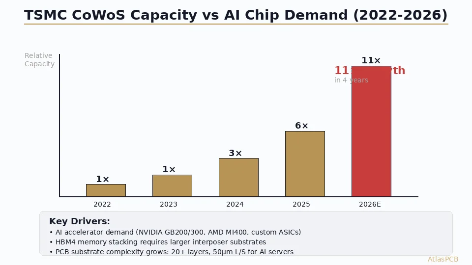
TSMC has unveiled sweeping capacity expansion plans at its annual Taiwan Technology Symposium, projecting a compound annual growth rate (CAGR) of 70% for 2nm and A16 wafer production from 2026 through 2028. The company simultaneously announced that CoWoS advanced packaging capacity will grow at over 80% CAGR from 2022 to 2027, underscoring the semiconductor industry’s accelerating shift toward advanced nodes and heterogeneous integration.
Nine Fabs and Packaging Plants in 2026
TSMC plans to build nine new fabrication facilities and packaging plants in 2026, spanning its global manufacturing footprint:
Arizona, USA:
- First fab: already in production
- Second fab: tool installation underway for the second half of 2026
- Third fab: construction in progress
- Fourth fab and a dedicated packaging facility: expected to break ground this year
- Arizona output projected to increase 1.8× year-over-year in 2026, with yields comparable to Taiwan operations
Japan:
- First fab: volume production at 22nm and 28nm nodes
- Second fab: plans upgraded from 7nm to 3nm in response to strong customer demand — a significant acceleration of Japan’s advanced node roadmap
Germany:
- Fab under construction, progressing on schedule
- Initial technology: 28nm and 22nm, followed by 16nm and 12nm
- Positions European automotive and industrial customers closer to advanced semiconductor supply
Advanced Packaging: The Real Bottleneck Story
While leading-edge node capacity grabs headlines, TSMC’s packaging technology announcements may have greater implications for the PCB and substrate supply chain:
SoIC (System on Integrated Chips):
- Now in mass production, delivering 56× higher interconnect density and 5× better energy efficiency compared to 2015-era CoWoS
- 6-micron bonding pitch version set for production in 2025
- N2-generation SoIC will support 6-micron stacking in 2028
- A14-generation planned for 4.5-micron bonding pitch
CoWoS (Chip on Wafer on Substrate):
- Current 5.5-reticle-size version achieving 98% yields
- A 14-reticle-size version capable of integrating 20 HBM stacks is planned for 2028
- An even larger version supporting 24 HBM stacks is targeted for 2029
System on Wafer (SoW):
- Can integrate up to 64 HBM stacks and 16 CoWoS modules at sizes exceeding 40 reticles
- SoWP entered mass production in 2024
- HBM-integrated SoWX targeted for 2029
COUPE (Compact Universal Photonic Engine):
- Delivered a 200 Gbps Micro Ring Modulator this year
- Claims 4× higher energy efficiency and 10× lower latency compared to copper interconnects
- Signals TSMC’s push into silicon photonics for data center interconnect
What This Means for PCB and Substrate Demand
TSMC’s capacity expansion has direct implications for PCB manufacturers and substrate suppliers:
1. Substrate complexity escalation: As CoWoS packages grow from 5.5 to 14 reticles, the organic substrates and interposers connecting these packages to the system board become correspondingly more complex. Multi-layer, ultra-fine-line substrates with 2/2 μm line/space are required — pushing fabrication capabilities beyond traditional PCB processes into [IC substrate territory]/blog/ic-substrate-vs-hdi-pcb-substrate-like-pcb-slp-technology/).
2. ABF substrate demand surge: Each CoWoS package requires high-end ABF (Ajinomoto Build-up Film) substrates. With CoWoS capacity growing 80%+ CAGR, demand for ABF material will continue to outstrip supply — consistent with the [ABF price increases already seen in 2026]/news/news-ajinomoto-abf-substrate-price-increase-2026/).
3. PCB-level thermal management: Larger packages dissipate more power. System boards supporting these advanced packages need enhanced [thermal via arrays]/blog/pcb-thermal-via-design/), thicker copper planes, and careful [power delivery network design]/blog/pcb-power-integrity-pdn-decoupling-design/) to handle 500W+ AI accelerator modules.
4. High-speed interconnect on motherboards: As chip-to-chip bandwidth increases with CoWoS and SoIC, the PCB traces connecting these modules must support higher data rates. Demand for [low-loss laminates like Megtron 7]/blog/mmwave-pcb-material-selection-rogers-megtron-lcp-5g-6g/) and controlled-impedance [HDI stackups]/blog/hdi-pcb-stackup-design-advanced/) will grow in parallel with TSMC’s packaging roadmap.
TSMC’s vision of a $1.5 trillion semiconductor market by 2030 implies a PCB and substrate market that must grow proportionally. For PCB fabricators and their customers, the message is clear: invest in advanced capability now, or risk being unable to serve the next generation of AI, HPC, and 5G/6G products.
Sources: Electronics Weekly (May 15, 2026), TSMC Taiwan Technology Symposium
Image: Alexandre Debiève via Unsplash
Working on next-gen server or AI hardware that needs advanced PCB substrates? AtlasPCB manufactures [HDI boards]/blog/hdi-pcb-stackup-design-advanced/) with laser-drilled microvias and fine-line capability for high-performance computing applications. Get a quote →
About AtlasPCB — We specialize in complex PCB manufacturing for HDI, RF, and high-reliability applications. Explore our RF and high-frequency PCB services, or get an impedance-controlled PCB manufacturing . Every order includes free engineering review. Get your quote.
Reviewed by AtlasPCB Engineering Team — IPC-certified manufacturing specialists with 15+ years of production experience in HDI, RF, and high-reliability PCB fabrication. Content based on factory floor data and real customer design reviews.
- news
- tsmc
- 2nm
- advanced-packaging
- cowos
- semiconductor
- 5g
- ai