· AtlasPCB Engineering · News · 4 min read
Siemens Launches Fuse EDA AI Agent: Autonomous Workflow Orchestration Across Semiconductor and PCB Design
Siemens has announced the Fuse EDA AI Agent, a purpose-built autonomous AI system that plans and orchestrates multi-tool workflows across semiconductor, 3D IC, and PCB system design — from schematic capture through manufacturing sign-off. The system integrates with NVIDIA Agent Toolkit and Nemotron models.
Siemens Introduces Autonomous AI Agent for End-to-End EDA Workflows
Siemens Digital Industries Software announced the Fuse EDA AI Agent on March 16, 2026 — a purpose-built autonomous AI system that plans, orchestrates, and executes complex workflows spanning semiconductor, 3D IC, and printed circuit board (PCB) design. The system represents a significant evolution from Siemens’ earlier in-tool AI capabilities (Fuse EDA AI system) to full end-to-end workflow automation.
Built on NVIDIA Agent Toolkit with support for advanced Nemotron models and NVIDIA AI infrastructure, the Fuse EDA AI Agent manages processes across Siemens’ comprehensive EDA portfolio, including the Xpedition PCB design platform and HyperLynx signal integrity tools.
Key Capabilities for PCB System Design
The Fuse EDA AI Agent covers the complete PCB system workflow through integration with Siemens’ design tools:
PCB Layout and Analysis (Xpedition):
- Automated placement optimization based on signal grouping and thermal constraints
- Routing orchestration for high-speed differential pairs and power distribution
- Signal integrity analysis automation through HyperLynx integration
- Design rule checking and constraint management across complex boards
Manufacturing Sign-off:
- Automated DFM (Design for Manufacturability) verification through Calibre integration
- Physical verification including DRC violation analysis and resolution
- Design-for-test (DFT) workflow management through Tessent integration
3D IC and Advanced Packaging:
- Power/ground load optimization for interposer designs
- Signal path plan clustering in Innovator3D IC software
- CoWoS and chiplet package interconnect optimization
How the Fuse AI Agent Works
Unlike generic AI assistants that provide suggestions, the Fuse EDA AI Agent operates as a domain-scoped autonomous agent that:
- Plans — Analyzes the design intent and creates an execution strategy across multiple tools
- Orchestrates — Manages the sequence of tool invocations, passing results between stages
- Executes — Directly drives EDA tools to perform design, verification, and analysis tasks
- Iterates — Reviews results against constraints and repeats steps if violations are detected
“We are delivering intelligent automation across the complete EDA lifecycle, enabling our customers to dramatically reduce design cycles while maintaining the highest quality standards,” said Amit Gupta, chief AI strategy officer at Siemens EDA. “Our open architecture allows customers to integrate their own workflows and models, providing the flexibility required for enterprise-scale AI deployment.”
Why Domain-Specific AI Matters for EDA
The announcement addresses a fundamental limitation of general-purpose AI in electronics design: standard AI tools lack the proprietary domain knowledge needed to interpret dense, physics-based EDA data. PCB design involves complex physical constraints — electromagnetic field interactions, thermal gradients, mechanical stress, and manufacturing process limitations — that generic AI cannot reason about effectively.
Siemens’ approach builds domain expertise directly into the AI agent through:
- Specialized parsers for EDA file formats (ODB++, Gerber, netlist, constraint files)
- Physics-aware reasoning about signal integrity, power integrity, and thermal effects
- Manufacturing knowledge about fabrication process capabilities and limitations
- EDA-specific data lake with multimodal understanding of schematics, layouts, and simulation results
Industry Context: The Race for AI-Powered EDA
Siemens’ announcement intensifies competition in AI-enhanced PCB and semiconductor design tools:
- Cadence has integrated ML-based optimization into Allegro for placement and routing guidance
- Quilter.ai offers fully autonomous PCB layout from schematic to DRC-clean design
- Flux raised $37 million in February 2026 for AI-driven PCB layout and firmware generation
- Altium has added AI-assisted routing and component selection features
- Synopsys uses ML for analog layout automation and yield optimization
The market is evolving from AI-as-assistant (suggesting improvements) to AI-as-agent (executing complete workflows autonomously). Siemens’ cross-tool orchestration approach is particularly significant because real PCB designs require coordination across 5–10 different specialized tools.
What This Means for Hardware Engineers
For PCB designers and engineering teams, the Fuse EDA AI Agent suggests several near-term impacts:
Accelerated design iteration:
- What currently takes 2–4 weeks of engineer time for placement-routing-verification cycles could compress to days
- More design variants explored in the same calendar time
Quality improvement:
- AI agents don’t skip verification steps or make shortcuts under schedule pressure
- Consistent application of design rules and manufacturing constraints
Skill accessibility:
- Junior engineers can leverage AI orchestration to produce designs meeting senior-level quality standards
- Complex multi-domain optimizations (SI + PI + thermal + DFM) become accessible without specialist expertise in each area
Implications for PCB manufacturers:
- Expect designs arriving for fabrication to have tighter DFM compliance
- AI-optimized designs may use manufacturing capabilities more aggressively (tighter trace/space, thinner dielectrics)
- Increased design complexity enabled by AI may drive demand for advanced fabrication capabilities
AtlasPCB Perspective
As AI-powered EDA tools enable engineers to push design boundaries further, PCB manufacturers must maintain capabilities that match the increasing design complexity. At AtlasPCB, we support the [advanced HDI fabrication]/blog/hdi-microvia-stacked-vs-staggered-reliability/), [tight impedance tolerances]/blog/controlled-impedance-pcb-design-stackup-calculations/), and [complex stackup designs]/blog/pcb-stackup-symmetry-balanced-lamination-warpage/) that AI-optimized boards increasingly demand.
We encourage designers using next-generation EDA tools to engage our engineering team early in the design process — our DFM review services ensure that AI-generated designs align with real-world fabrication constraints before they reach production.
Source: Siemens News (March 16, 2026), PR Newswire
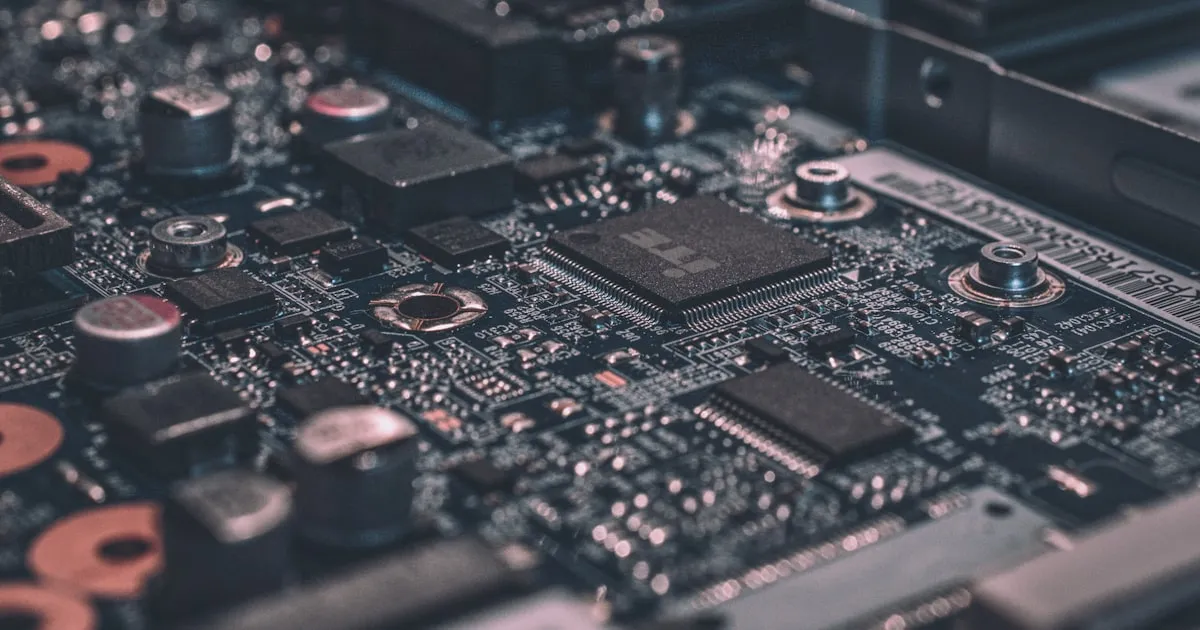
Image: Vishnu Mohanan via Unsplash
About AtlasPCB — We specialize in complex PCB manufacturing for HDI, RF, and high-reliability applications. Explore our impedance-controlled PCB manufacturing . Every order includes free engineering review. Get your quote.
Reviewed by AtlasPCB Engineering Team — IPC-certified manufacturing specialists with 15+ years of production experience in HDI, RF, and high-reliability PCB fabrication. Content based on factory floor data and real customer design reviews.
- news
- Siemens
- Fuse EDA
- AI agent
- PCB design
- EDA
- semiconductor
- 3D IC
- NVIDIA
- design automation
- Xpedition
- signal integrity