· AtlasPCB Engineering · News · 5 min read
Siemens Wins Chiplet Summit 2026 Best of Show for 3D IC Packaging Design — EDA Tools Reshape PCB-Package Co-Design
Siemens EDA wins 'Packaging: Design' Best of Show at Chiplet Summit 2026 for Innovator3D IC, a unified flow for heterogeneous chiplet integration across 2.5D/3D packaging. The award signals growing EDA investment in PCB-package co-design as multi-die systems demand end-to-end design continuity.

The tools that engineers use to design PCBs and semiconductor packages are converging—and Siemens just won a major industry award for accelerating that convergence. At the 2026 Chiplet Summit held at the Santa Clara Convention Center, Siemens EDA took the “Packaging: Design” Best of Show Award for its Innovator3D IC™ solution, which provides unified pathfinding, planning, and heterogeneous integration of chiplets across advanced 2.5D and 3D packaging technologies.
Source: Siemens Press Release, February 19, 2026
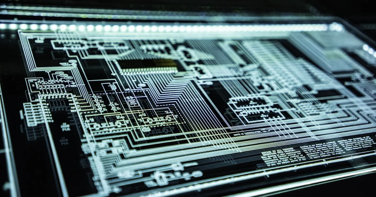
What Innovator3D IC Actually Does
Traditional semiconductor package design has been fragmented—die designers work in one tool, package substrate designers in another, and PCB designers in yet another. This fragmentation creates integration problems that aren’t discovered until late in the design cycle, when changes are expensive.
Innovator3D IC attempts to solve this by providing a system-level design environment where multiple die, chiplets, interposers, and packages are optimized and validated within a single unified flow:
- Pathfinding: Early-stage exploration of chiplet placement, interconnect routing, and packaging technology selection before committing to detailed design
- Planning: Floor-planning multiple die on shared substrates/interposers with real physical constraints
- Heterogeneous integration: Managing different die technologies (logic, memory, analog, RF) with different process nodes on a single package
- Validation: Cross-domain checking between die-level, package-level, and board-level design rules
“The recognition of Innovator3D IC at Chiplet Summit reinforces our mission to deliver cutting-edge technologies that radically accelerate how our customers develop next-generation semiconductors,” said AJ Incorvaia, senior vice president of Electronic Board Systems at Siemens Digital Industries Software.
Why This Matters for PCB Engineers
You might think chiplet design tools are purely a semiconductor concern. They’re not. Here’s why this matters for PCB design:
The Design Boundary Is Moving
As chiplet packages grow larger and more complex, they absorb functionality that previously existed at the PCB level:
- Power regulation moved into package (embedded voltage regulators)
- Passive components embedded in package substrates
- High-speed interconnect shortened by co-packaging (CXL, PCIe)
- Memory integrated at package level (HBM, LPDDR on interposer)
PCB designers increasingly need to understand package-level constraints because they directly affect board-level requirements—power delivery, signal breakout, thermal management.
Co-Design Is Now Mandatory
You can no longer design a PCB independently from the packages it hosts. Modern co-design requirements include:
Simultaneous BGA escape: Package ball map and PCB routing must be co-optimized—the package designer places balls where PCB routing is possible, not arbitrary.
Power delivery co-simulation: PDN analysis must span die → package substrate → PCB, simulating impedance continuously from silicon to bulk capacitors.
Signal integrity end-to-end: Channel simulations for 112G PAM4 must include die driver model → package trace → via transition → PCB trace → via → connector, all in one simulation.
Thermal co-design: Package thermal solution and PCB thermal vias/copper area must be designed together to achieve system thermal targets.
EDA Tool Convergence
The Chiplet Summit award reflects a broader EDA industry trend:
- Cadence: Integrity 3D-IC platform for cross-domain design
- Synopsys: 3DIC Compiler for multi-die integration
- Siemens: Innovator3D IC (award winner) for packaging pathfinding
- Ansys: RedHawk-SC and Icepak for power/thermal co-simulation
These tools are moving from pure semiconductor focus toward system-level integration that includes PCB design. Engineers who work exclusively in PCB tools (Altium, KiCad, OrCAD) will increasingly need interface knowledge with package-level EDA.
The Chiplet Summit 2026 Context
The fourth annual Chiplet Summit has grown significantly, reflecting the industry’s rapid adoption of multi-die architectures:
Key themes from the event:
- UCIe (Universal Chiplet Interconnect Express) ecosystem maturation
- Heterogeneous integration manufacturing challenges
- Known-good-die testing methodologies
- Thermal management of multi-chiplet packages
- Supply chain considerations for multi-vendor chiplet sourcing
“As multi-die integration grows more complex, this solution gives designers the tools to move faster and innovate with confidence,” said Chuck Sobey, general chair of the Chiplet Summit.
The event serves technologists who use chiplets in designs for processors, memories, communications chips, and AI devices—representing the fastest-growing segment of the semiconductor industry.
TSMC’s Packaging Ecosystem: The Backdrop
The Siemens award comes against the backdrop of TSMC’s aggressive packaging technology roadmap:
- A16 (1.6nm): Production planned for late 2026 with backside power delivery
- CoWoS-L: Extended interposer size for larger AI accelerator packages
- SoIC: True 3D chip stacking with sub-10μm bump pitch
- InFO-AiP: Fan-out packaging for 5G mmWave antenna integration
Each of these packaging technologies creates new challenges for the PCB that hosts the package—challenges that require the kind of co-design tools Siemens is developing.
Source: EE News Europe, 2026
Implications for System Design Teams
Organizational Changes
Companies designing chiplet-based products are restructuring teams:
- Package design is moving from an afterthought to a first-class design discipline
- PCB-package co-design roles are emerging (hybrid expertise)
- System architects now need packaging knowledge alongside digital/analog expertise
- Thermal engineers work across die, package, and board simultaneously
Skill Requirements
Engineers entering the PCB field should invest in understanding:
- Advanced packaging technologies (fan-out, 2.5D, 3D)
- Package substrate design rules and manufacturing constraints
- Multi-physics simulation (electrical + thermal + mechanical)
- Cross-domain data exchange formats (IEEE 2401, ODB++)
Design Timeline Impact
Chiplet-based designs have longer package development cycles:
- Package concept: 12-18 months before production
- Substrate design: 6-12 months
- PCB design: 4-8 months
- System integration: 3-6 months
PCB designers who engage early in the package design phase can influence ball maps, escape routing, and power/ground distribution to simplify their own work later.
AtlasPCB Perspective: Supporting Complex Package Integration
The chiplet revolution increases demand for PCB manufacturing excellence at the board level:
- Finer BGA escape routing: Chiplet packages use finer ball pitches, requiring tighter PCB design rules
- Higher layer counts: More signals, more power domains = more routing and plane layers
- Tighter impedance control: High-speed die-to-die links demand ±5% impedance matching
- Better planarity: Large packages require PCB surface flatness for reliable BGA attachment
- Advanced materials: Low-loss laminates for maintaining signal integrity at 56+ Gbps
As the EDA tools improve to enable better co-design, the PCBs that emerge from these unified flows will push manufacturing capabilities—exactly where AtlasPCB focuses its technology investment.
Designing PCBs for advanced chiplet-based packages? AtlasPCB provides high-layer-count HDI manufacturing with the dimensional precision and impedance control required for modern semiconductor packaging. Get a quote to discuss your advanced design requirements.
About AtlasPCB — We specialize in complex PCB manufacturing for HDI, RF, and high-reliability applications. Explore our full PCB manufacturing capabilities, or get an instant online quote . Every order includes free engineering review. Get your quote.
Reviewed by AtlasPCB Engineering Team — IPC-certified manufacturing specialists with 15+ years of production experience in HDI, RF, and high-reliability PCB fabrication. Content based on factory floor data and real customer design reviews.
- industry news
- chiplet
- 3D IC
- Siemens EDA
- advanced packaging
- PCB design
- heterogeneous integration
- 2.5D packaging