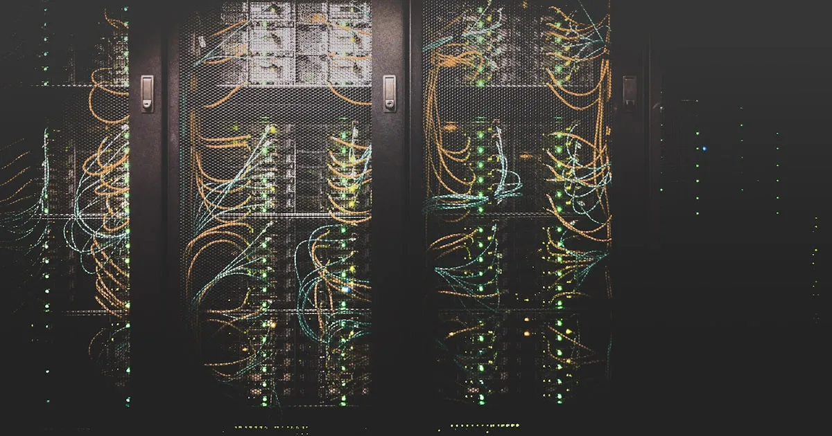
· AtlasPCB Engineering · News · 4 min read
Semiconductor Materials Market Hits Record $73.2 Billion in 2025, Driven by Advanced Packaging
SEMI reports global semiconductor materials revenue grew 6.8% YoY to $73.2 billion in 2025, with packaging materials up 9.3% as advanced substrate and bonding wire demand surges. Taiwan leads at $21.7B for 16th consecutive year.

SEMI Reports Record Materials Revenue
The global semiconductor materials market reached a record $73.2 billion in revenue during 2025, representing 6.8% year-over-year growth, according to data published May 12, 2026 by SEMI in its Materials Market Data Subscription (MMDS).
The growth was driven by gains in both wafer fabrication and packaging materials segments, reflecting increasing process complexity at advanced nodes and sustained investment in high-performance computing and high-bandwidth memory manufacturing.
Source: SEMI Materials Market Data Subscription, May 2026 | iConnect007 Coverage
Key Market Segments
Wafer Fabrication Materials: $45.8 Billion (+5.4%)
Wafer fab materials grew 5.4% to $45.8 billion, driven by:
- Lithography materials (photomasks, photoresist, ancillaries): Double-digit growth as EUV adoption expands
- Wet chemicals: Strong growth from higher process intensity at sub-5nm nodes
- CMP slurries: Increased planarization steps in advanced logic and 3D NAND
- Process gases: Higher consumption per wafer at leading-edge fabs
The growth reflects a fundamental trend: each new technology node requires more processing steps and more materials per wafer. A 3nm logic wafer consumes approximately 30% more materials than a 7nm wafer.
Packaging Materials: $27.4 Billion (+9.3%)
Packaging materials outpaced fab materials with 9.3% growth to $27.4 billion:
- Substrates: Leading growth driver, fueled by demand for advanced ABF (Ajinomoto Build-up Film) substrates used in AI GPU and HPC packaging
- Bonding wire: Revenue boosted by higher gold prices and increased wire bonding volume for automotive and IoT devices
- Underfill and encapsulants: Growing with flip-chip and advanced packaging adoption
- Lead frames: Steady growth in automotive power semiconductor packaging
The packaging materials segment’s faster growth rate signals the industry’s shift toward advanced packaging as a performance scaling vector, complementing traditional transistor shrinking.
Regional Market Share
| Region | Revenue (2025) | YoY Growth | Notes |
|---|---|---|---|
| Taiwan | $21.7B | Moderate | #1 for 16th consecutive year |
| China | $15.6B | Double-digit | Strongest growth among major regions |
| South Korea | $11.2B | Positive | Memory-driven demand |
| Japan | ~$8B (est.) | Positive | Specialty materials strength |
| North America | ~$7B (est.) | Double-digit | Advanced fab construction |
| Europe | Declined | Negative | Only region with YoY decrease |
Taiwan’s continued dominance reflects TSMC’s concentration of advanced-node manufacturing. China’s strong double-digit growth correlates with aggressive domestic fab expansion, including multiple new 28nm and 14nm facilities coming online in 2024-2025.
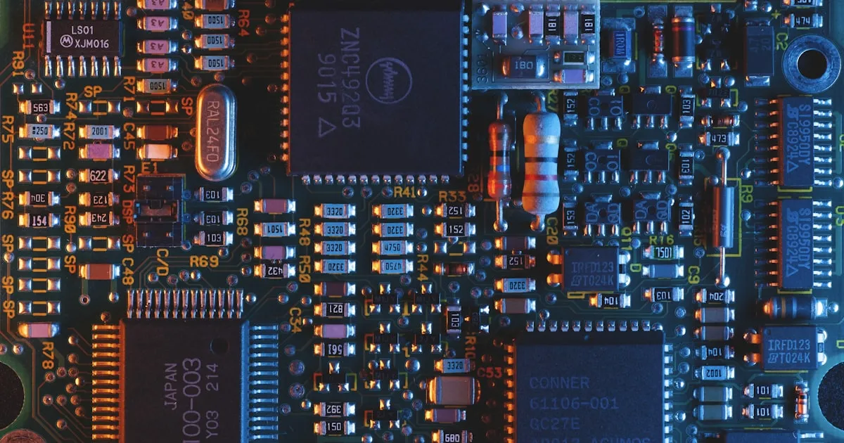
What This Means for the PCB Industry
The semiconductor materials market’s record performance has direct implications for PCB manufacturers and designers:
1. Substrate Demand Pressures PCB Materials Supply
ABF substrates—the critical interface between chips and PCBs—are consuming increasing amounts of laminate-grade materials. With substrate revenue growing at double-digit rates, competition for high-performance laminate raw materials (glass fabric, resin systems) intensifies across the supply chain.
2. Advanced Packaging Drives Board-Level Complexity
As chips move to advanced packages (chiplets, 2.5D/3D integration, fan-out wafer-level packaging), the host PCB must accommodate:
- Higher pin counts (4,000+ for AI accelerators)
- Tighter BGA pitches (0.4mm and below)
- More stringent impedance control requirements
- Better power delivery network design
3. Regional Shifts Affect Sourcing
China’s rapid growth in semiconductor manufacturing creates new local demand for PCB fabrication capacity, potentially tightening availability for export-oriented PCB orders in the region.
Material Category Breakdown
SEMI’s MMDS tracks semiconductor materials across multiple categories. The key growth drivers in 2025 included:
Wafer Fab Materials by Category
- Photomasks: Double-digit growth driven by EUV reticle complexity and cost
- Photoresist & ancillaries: Strong growth as multi-patterning increases resist consumption
- Process gases: Higher volumes per wafer at advanced nodes (atomic-layer processes)
- Wet chemicals: Growing with advanced cleaning requirements
- CMP slurries/pads: More planarization steps at 3nm and below
- Sputtering targets: Steady growth with new metal interconnect schemes
Packaging Materials by Category
- Organic substrates (ABF, BT): Fastest growth, driven by AI chip packaging
- Bonding wire: Revenue boosted by gold price increases
- Lead frames: Automotive semiconductor volume growth
- Mold compounds: Advanced encapsulants for 3D packaging
- Underfill materials: Flip-chip adoption expanding
Historical Context
The $73.2 billion figure represents a return to growth after a slight correction in 2023:
| Year | Revenue | YoY Change |
|---|---|---|
| 2021 | $64.3B | +15.9% |
| 2022 | $72.7B | +13.0% |
| 2023 | $66.7B | -8.2% |
| 2024 | $68.5B | +2.7% |
| 2025 | $73.2B | +6.8% |
The 2023 correction reflected the post-pandemic demand normalization, while the 2024-2025 recovery tracks directly with AI-driven manufacturing ramp.
Market Outlook
With SEMI’s data confirming strong 2025 growth and Deloitte forecasting the semiconductor industry reaching $975 billion in total sales by 2026, materials demand is expected to continue climbing. The AI infrastructure buildout—requiring massive quantities of HBM, advanced logic chips, and high-performance networking ASICs—will keep substrate and packaging material consumption elevated through at least 2027.
For PCB designers and buyers, the key takeaway is that supply chain competition for advanced materials is intensifying. Lead times for high-layer-count boards using premium laminates may extend as substrate manufacturers compete for the same material inputs. Planning ahead and securing material allocation early in the design cycle is increasingly important for production programs.
The SEMI Materials Market Data Subscription provides annual revenue data with 10 years of historical context and two-year forecasts, covering seven global regions.
About AtlasPCB — We specialize in complex PCB manufacturing for HDI, RF, and high-reliability applications. Explore our impedance-controlled PCB manufacturing . Every order includes free engineering review. Get your quote.
Reviewed by AtlasPCB Engineering Team — IPC-certified manufacturing specialists with 15+ years of production experience in HDI, RF, and high-reliability PCB fabrication. Content based on factory floor data and real customer design reviews.
- news
- semiconductor
- materials-market
- advanced-packaging
- pcb-substrates