· AtlasPCB Engineering · News · 4 min read
Global Semiconductor Industry on Track for $975 Billion in 2026, AI Drives Historic PCB Demand
Deloitte forecasts semiconductor sales reaching $975 billion in 2026 with 26% growth. The AI infrastructure boom creates unprecedented demand for advanced PCBs, substrates, and high-layer-count boards used in data center networking.
Semiconductor Industry Approaches $1 Trillion Milestone
The global semiconductor industry is projected to reach $975 billion in annual sales during 2026, representing a historic peak driven by the intensifying AI infrastructure buildout, according to Deloitte’s 2026 Semiconductor Industry Outlook. This follows record-setting 2025 sales of $795.6 billion (26.2% year-over-year growth).
The Semiconductor Industry Association (SIA) confirmed this trajectory with January 2026 monthly sales of $82.5 billion—a staggering 46.1% increase from January 2025—suggesting the full-year forecast may prove conservative.
Sources: Deloitte 2026 Semiconductor Industry Outlook | Semiconductor Industry Association
AI Infrastructure: The Growth Engine
The primary driver behind this unprecedented growth is AI infrastructure spending:
Data Center GPU Demand
- NVIDIA, AMD, and Intel shipping millions of AI accelerators annually
- Each AI GPU requires a high-layer-count substrate (16-20+ layers) and accompanying PCB ecosystem
- Training clusters scaling from thousands to hundreds of thousands of GPUs per deployment
High-Bandwidth Memory (HBM)
- HBM3e production ramping aggressively at SK Hynix, Samsung, and Micron
- Each HBM stack requires advanced interposer and substrate technology
- HBM revenue expected to exceed $30 billion in 2026
Networking ASICs
- 800G and 1.6T Ethernet switching demands ultra-high-layer PCBs
- Broadcom, Marvell, and custom Silicon competing for advanced packaging capacity
- Network switch boards using 20-30 layer PCBs with HDI technology
Impact on PCB Industry
1. Advanced Board Demand at All-Time High
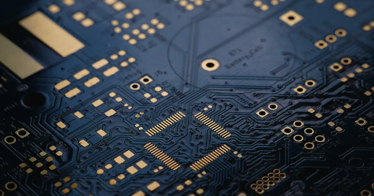
AI server motherboards represent the most complex PCBs in volume production:
- Layer counts: 16-28 layers (standard server: 8-12 layers)
- Materials: Low-loss laminates (Megtron 6/7, TU-872) mandatory for 112Gbps SerDes
- Impedance control: ±5% tolerance on 85Ω differential pairs
- Board size: 600×450mm and larger for GPU baseboard
2. Supply Chain Bottlenecks
With the industry approaching $1 trillion, every segment faces capacity constraints:
| Component | Constraint | Lead Time Impact |
|---|---|---|
| ABF substrates | Ajinomoto film supply | +4-8 weeks |
| High-layer PCBs | Lamination press capacity | +2-4 weeks |
| Low-loss laminates | Resin production limits | +2-3 weeks |
| HDI drilling | Laser drill machine availability | +1-2 weeks |
| Advanced testing | TDR and VNA equipment | +1 week |
3. PCB Technology Requirements Escalating
AI hardware is pushing PCB technology boundaries:
Signal integrity requirements:
- 224Gbps PAM4 signaling requires insertion loss <0.5dB/inch at 56GHz
- Crosstalk isolation demands wider trace spacing and ground shielding
- Power delivery requires thick copper (2-4oz) with fine-line signal routing on same board
Thermal management:
- 700W+ GPU TDP requires PCB-integrated thermal solutions
- Embedded copper coin and heavy copper planes for heat spreading
- Thermal via arrays under high-power components
Manufacturing precision:
- Registration accuracy: ±25μm layer-to-layer for HDI
- Drilling accuracy: ±12.5μm for stacked microvias
- Impedance control: ±5% at 56+ GHz operating frequency
Regional Investment Landscape
North America: Reshoring Momentum
The CHIPS Act and commercial demand are driving significant domestic investment:
- Intel, TSMC, Samsung building fabs in Arizona, Ohio, Texas
- Corresponding demand for local PCB supply chain
- Advanced substrate manufacturing pilot lines under development
Asia-Pacific: Capacity Leaders
- Taiwan remains the manufacturing center for advanced semiconductors and substrates
- South Korea investing heavily in HBM and advanced packaging
- China expanding at mature nodes with growing domestic PCB demand
Europe: Strategic Materials Focus
- AT&S investing in advanced substrate capability in Austria
- ASML equipment demand at record levels
- Focus on automotive semiconductor self-sufficiency
Market Projections Through 2030
| Year | Projected Revenue | Growth Rate | Key Driver |
|---|---|---|---|
| 2025 | $795.6B (actual) | 26.2% | AI training ramp |
| 2026 | $975B | 22-26% | AI inference scaling |
| 2027 | $1.1-1.2T (est.) | 15-20% | Edge AI + automotive |
| 2030 | $2.0T (est.) | CAGR ~20% | Ubiquitous AI |
If current growth rates hold, the semiconductor industry is on track to become a $2 trillion market by the mid-2030s—with corresponding demand for PCBs, substrates, and packaging materials at every level.
What This Means for PCB Buyers
Short-Term (2026)
- Extended lead times for high-layer-count boards using premium materials
- Pricing pressure on low-loss laminates and ABF substrates
- Allocation risk for boards competing with AI/data center programs
Medium-Term (2027-2028)
- New capacity coming online may ease constraints
- Technology advancement with SAP/mSAP processes enabling finer features on standard equipment
- Alternative materials being qualified for cost-sensitive applications
Design Recommendations
- Lock in materials early when designing for volume production
- Design with standard materials where possible (avoid sole-sourced exotics)
- Consider manufacturing location based on regional capacity and capabilities
- Engage fabricators early in the design process for material availability guidance
The $1 Trillion Question
As the semiconductor industry crosses the trillion-dollar threshold, the supporting infrastructure—including PCB fabrication—must scale proportionally. Board-level interconnect represents roughly 2-3% of total semiconductor value chain, suggesting the global PCB market (currently ~$90 billion) will need to reach $100-120 billion by 2028 to avoid becoming a bottleneck.
For PCB manufacturers investing in advanced capability (ultra-high-layer, sub-50μm features, low-loss materials), the growth outlook is exceptionally strong. For buyers, the key is securing supply chain partnerships that provide access to this constrained capacity.
AtlasPCB provides advanced-technology PCB manufacturing services including high-layer-count boards, controlled impedance, and HDI technology for AI and data center applications. Request a quote for your high-performance design.
About AtlasPCB — We specialize in complex PCB manufacturing for HDI, RF, and high-reliability applications. Explore our impedance-controlled PCB manufacturing . Every order includes free engineering review. Get your quote.
Reviewed by AtlasPCB Engineering Team — IPC-certified manufacturing specialists with 15+ years of production experience in HDI, RF, and high-reliability PCB fabrication. Content based on factory floor data and real customer design reviews.
- news
- semiconductor-market
- ai-infrastructure
- data-center
- pcb-demand
- market-forecast