· AtlasPCB Engineering · News · 3 min read
SEMICON SEA 2026: Chinese PCB Companies Pivot to Advanced Packaging as 95+ Firms Showcase in Singapore
SEMICON Southeast Asia 2026 drew over 95 mainland Chinese exhibitors, signaling a major shift from traditional PCB manufacturing toward advanced semiconductor packaging, IC substrates, and AI-driven assembly solutions.
The fifth edition of SEMICON Southeast Asia, held May 5-7, 2026 at the MITEC Exhibition Centre in Kuala Lumpur, marked a turning point for the PCB industry’s relationship with advanced semiconductor packaging. Over 95 mainland Chinese companies exhibited at this year’s show — a record participation level that reflects the industry’s accelerating pivot from traditional PCB fabrication toward wafer-level packaging, IC substrates, and semiconductor-grade manufacturing.
From PCB to Advanced Packaging
The most notable trend among Chinese exhibitors was a wholesale repositioning away from “PCB manufacturer” branding toward semiconductor-oriented positioning. Companies from Shenzhen, Dongguan, Suzhou, and Shanghai dominated the exhibitor list, spanning semiconductor equipment, advanced packaging materials, IC substrates, cleanroom solutions, and precision automation.
Key exhibitors included Guangdong Taijin Semiconductor Technology, QUICK Semiconductor Technology, SiCentury Semiconductor Technology (Suzhou), and Macrotest Semiconductor Technology — many of which evolved from traditional PCB supply chain origins.
According to IC&PCB Union’s analysis of the event, the word “Semiconductor” has become a core keyword in Chinese company names, reflecting “the industry’s transition from traditional electronics manufacturing toward advanced packaging and wafer-level technologies.”
PCB Equipment Suppliers Enter Semiconductor Markets
While SEMICON SEA is not traditionally a PCB-focused exhibition, multiple Chinese PCB equipment and materials companies actively participated. Representatives included Dongguan Allmerit Technology, Wuxi KINGWIN Electronic Equipment, Shenzhen Tensun Precision Equipment, and Chip Shine Electronics Technology.
These companies are leveraging their PCB process expertise — in areas like laser drilling, plating, imaging, and wet processing — to address adjacent semiconductor packaging requirements where similar process technologies apply at finer geometries.
Delta Electronics Highlights AI in Packaging
In a parallel announcement, Delta Electronics presented its AI-integrated smart manufacturing solutions at the show. The company’s booth demonstrated how artificial intelligence enables “smarter, more connected, advanced semiconductor packaging production featuring greater speed, precision, and scalability,” according to their press release.
Delta’s presentation focused on power management and thermal solutions for advanced packaging production equipment — areas directly relevant to high-density PCB fabrication where similar thermal challenges exist.
ASMPT Showcases Full-Spectrum Solutions
ASMPT, under the theme “Empower the Intelligence Revolution,” exhibited semiconductor packaging, SMT assembly, and intelligent factory technologies targeting AI, Smart Mobility, and Hyperconnectivity applications. Their booth covered the full spectrum from die bonding to PCB assembly.
What This Means for PCB Engineers
The convergence of PCB and semiconductor packaging creates both challenges and opportunities:
- Substrate requirements are blurring — IC substrates use PCB manufacturing techniques (SAP/mSAP processes) at semiconductor tolerances
- Equipment is crossing over — Laser drill, plating, and inspection equipment designed for PCB is being adapted for packaging substrates
- Materials overlap — ABF build-up films, low-CTE glass cloth, and ultra-thin copper foils serve both markets
- Engineering talent is shared — PCB design skills translate directly to substrate design
For hardware engineers sourcing advanced substrates and HDI boards, this convergence means more fabricators are developing capabilities that bridge the gap between traditional multilayer PCBs and semiconductor-grade substrates.
AtlasPCB’s Position
At AtlasPCB, we’ve been investing in advanced HDI capabilities that overlap with IC substrate manufacturing — including mSAP processing for ≤30 μm trace/space, any-layer microvia technology, and ultra-thin core handling. As the line between PCBs and packaging substrates continues to blur, our manufacturing platform is positioned to serve both markets.
Explore Our HDI Capabilities → | Request a Quote →
Sources: IC&PCB Union, ASMPT Press Release, Delta Electronics / PRNewswire
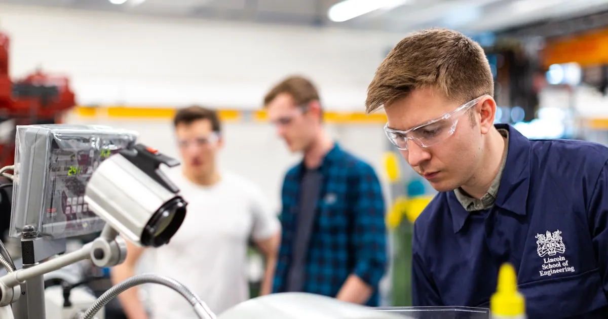
Image: ThisisEngineering via Unsplash
About AtlasPCB — We specialize in complex PCB manufacturing for HDI, RF, and high-reliability applications. Explore our impedance-controlled PCB manufacturing . Every order includes free engineering review. Get your quote.
Reviewed by AtlasPCB Engineering Team — IPC-certified manufacturing specialists with 15+ years of production experience in HDI, RF, and high-reliability PCB fabrication. Content based on factory floor data and real customer design reviews.
- news
- semicon sea
- advanced packaging
- ic substrate
- pcb industry
- semiconductor
- china