· AtlasPCB Engineering · News · 6 min read
Samsung 2nm Yields Reach 55% as Gate-All-Around Production Ramps — PCB Substrate Demands Intensify
Samsung's 2nm GAA process yields have improved from 20-30% to 55%, signaling imminent mass production for AI and mobile chips. The advancement drives new PCB substrate requirements including ultra-fine-line IC substrates and advanced packaging interposers.
Samsung Electronics’ advanced 2nm Gate-All-Around (GAA) process has achieved yield rates of approximately 55%, according to reports from Korean media outlet Busan Ilbo cited by TrendForce. This represents a dramatic improvement from the 20-30% yields reported in H2 2025, signaling that mass production for commercial chips is approaching viability.
The development has significant implications for PCB and IC substrate manufacturers, as 2nm-class chips demand the most advanced packaging technologies—CoWoS, chip-on-wafer-on-PCB (CoWoP), and fan-out wafer-level packaging—all of which require ultra-high-density substrates that push manufacturing precision to its limits.
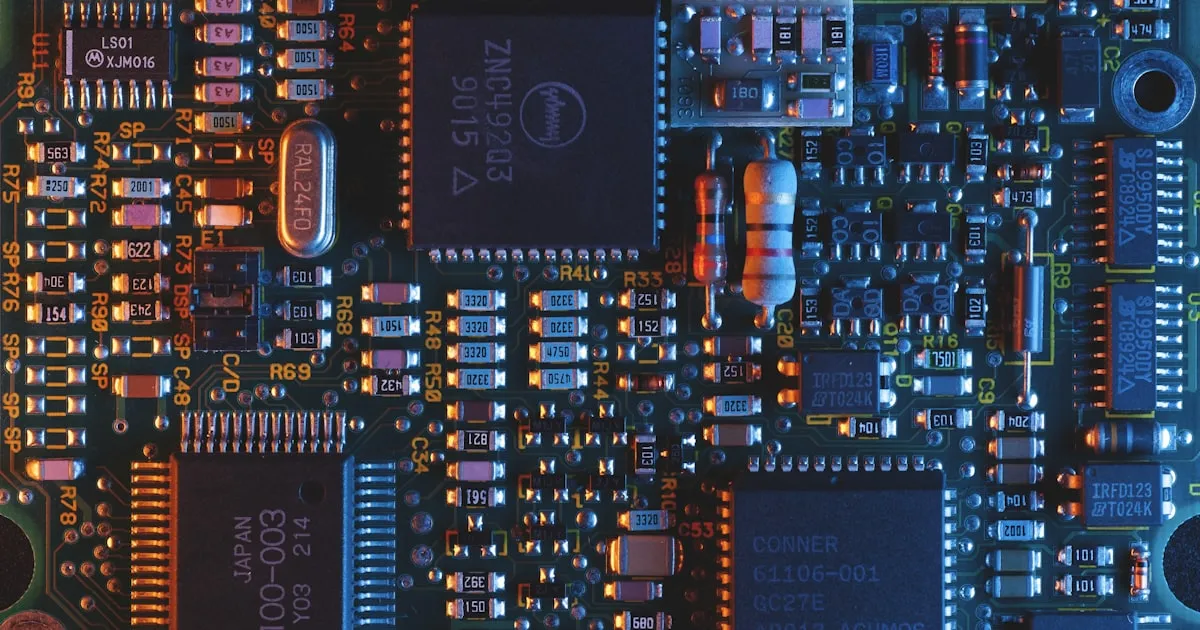
Source: Electronics Weekly, April 2026
The 2nm Yield Breakthrough
What 55% Yield Means
For advanced semiconductor nodes, 55% yield is a critical inflection point:
- Below 40%: Research/engineering phase—usable for small-die test chips but economically unviable for commercial products
- 40-55%: Early production possible for premium products where high ASP justifies lower yield (AI accelerators, flagship mobile SoCs)
- 55-70%: Commercial mass production viable for high-volume products
- Above 70%: Mature production—standard for volume manufacturing
Samsung’s progression from ~25% to 55% in roughly 6 months represents faster-than-expected learning curve acceleration. Industry analysts now expect first commercial 2nm GAA products in late 2026 or early 2027.
The Musk Factor
In July 2025, Elon Musk placed a $16 billion order with Samsung that included access to Samsung’s Taylor and Austin fabs in Texas. The order—reportedly for xAI’s next-generation AI training chips—provided Samsung with both the financial resources and the customer urgency to accelerate 2nm development.
Samsung is now competing directly with TSMC (which offers its own 2nm N2 process using nanosheet GAA transistors) for the AI accelerator market—the most lucrative segment in semiconductor manufacturing.
Impact on PCB and IC Substrate Technology
Why 2nm Chips Need Better Substrates
As transistor dimensions shrink, the performance bottleneck shifts from the die itself to the package and substrate. A 2nm chip with billions of transistors and thousands of I/O signals requires:
Higher I/O density: 2nm SoCs target 5,000-10,000+ package pins Finer redistribution lines: L/S (line/space) of 2/2μm to 5/5μm on IC substrates Lower loss materials: Signal frequencies exceeding 20 GHz require ultra-low Dk/Df substrates Larger interposers: Multi-chiplet designs requiring 2,000-3,000mm² silicon or organic interposers Tighter tolerances: Layer registration ±3μm, via position ±2μm
IC Substrate Manufacturing Challenges
The substrate requirements for 2nm chips push PCB-based manufacturing to its absolute limits:
Line/space capability:
- Current production: 8/8μm (advanced) to 15/15μm (standard)
- 2nm chip requirement: 2/2μm to 5/5μm in redistribution layers
- Gap: Requires semiconductor-like lithography in PCB fabs
Via technology:
- Current: 40-75μm laser-drilled microvias
- 2nm requirement: 10-25μm vias with 0.5:1 aspect ratio fill
- Solution: Semi-additive process (SAP) and modified semi-additive process (mSAP)
Material requirements:
- Ultra-low loss build-up films (Df <0.002 at 20 GHz)
- Low CTE glass core substrates (3-5 ppm/°C matching silicon)
- Ultra-thin dielectric layers (5-15μm build-up per layer)
Market Demand for Advanced Substrates
The AI boom is already straining IC substrate capacity:
- ABF substrate (Ajinomoto Build-up Film): Demand exceeds supply by 15-20% through 2027
- Glass core substrates: Emerging technology for next-gen interposers (Intel, Samsung investing)
- Organic interposers: Bridge technology between silicon and traditional organic substrates
- Fan-out panel-level packaging (FOPLP): Samsung and TSMC scaling for AI chip packaging
Prismark estimates the IC substrate market will grow from $15.8 billion (2025) to $22 billion (2027), with the AI/HPC segment representing over 40% of revenue growth.
Competitive Landscape: Samsung vs TSMC vs Intel
Process Technology Race
| Company | 2nm Node Name | Architecture | Target Production | Key Customer |
|---|---|---|---|---|
| Samsung | SF2 | GAA (MBCFET) | Late 2026 / Early 2027 | xAI (Musk) |
| TSMC | N2 | GAA (Nanosheet) | H2 2025 (limited) / H1 2026 (volume) | Apple, NVIDIA |
| Intel | Intel 18A | RibbonFET (GAA) + PowerVia | 2025 (delayed) | Internal + Terafab |
Packaging Technology Differentiation
The real competition is increasingly in packaging—not just transistors:
TSMC CoWoS: Dominant for AI GPUs (NVIDIA H200, B200). Capacity expanded 2.5× in 2025 but still insufficient for demand.
Samsung I-Cube4: Advanced 2.5D packaging competing with CoWoS. Integration with Musk’s Terafab for AI chip packaging.
Intel Foveros/EMIB: 3D stacking technology. Partnering with Musk for Intel 18A + Terafab integration announced April 2026.
What Intel’s Terafab Partnership Means
Electronics Weekly reported in April 2026 that Intel has partnered with Musk’s Terafab for co-development of advanced packaging. This suggests:
- Multi-source strategy for AI chips (xAI not solely dependent on Samsung)
- Advanced packaging becoming the critical differentiator (not just node shrink)
- Massive investment flowing into substrate and interposer manufacturing capacity
Implications for PCB Engineers and Designers
Board-Level Design Evolution
As chip packaging becomes more complex, the motherboard PCB must evolve:
Higher pin-count BGA support:
- 2nm chip packages will feature 5,000-10,000+ balls
- Ball pitch reducing from 0.8mm to 0.4-0.5mm
- Requires HDI substrate with 50/50μm or finer line/space for BGA escape routing
Power delivery challenges:
- 2nm chips at 3-5nm transistor density may consume 300-500W per die
- Current delivery of 500A+ requires ultra-low-impedance power planes
- Multiple voltage rails (0.6V, 0.75V, 1.0V, 1.8V) with tight regulation
Signal integrity at system level:
- Die-to-die communication at 112 Gbps PAM4 through package and board
- PCIe Gen6 (64 GT/s) requiring insertion loss budgets under 25 dB
- DDR6 interfaces operating at 12,800 MT/s with 0.4V signaling
Supply Chain Considerations
Hardware companies should prepare for tighter substrate availability:
- Book IC substrates 6-9 months ahead for advanced packaging designs
- Qualify alternative substrate vendors to avoid single-source dependency
- Design for multiple packaging options where possible (allow for both organic and silicon interposer variants)
- Monitor Samsung/TSMC capacity announcements for production timeline clarity
AtlasPCB’s Advanced Substrate Capabilities
HDI and mSAP Technology
AtlasPCB’s manufacturing capabilities support the board-level requirements of advanced chip packages:
Fine-line HDI:
- Line/space capability: 40/40μm production, 30/30μm pilot
- Microvia: 50μm laser-drilled, copper-filled, stacked up to 4 layers
- Layer count: Up to 32 layers with sequential lamination
- Registration: ±15μm layer-to-layer alignment
High-speed signal support:
- Low-loss laminate processing (Megtron 6/7, Tachyon 100G)
- Controlled impedance: ±5% tolerance verified by TDR
- Back-drill capability: ≤50μm stub length for 56+ Gbps signaling
- Mixed-dielectric constructions: RF + digital on single board
Package-Board Co-Design Services
Engineering support for designs targeting 2nm-class chips:
- BGA escape routing optimization for ultra-fine-pitch packages
- Power delivery network simulation and optimization
- Signal integrity analysis for next-gen interfaces (PCIe Gen6, DDR6, UCIe)
- Thermal simulation for high-power AI processor boards
Looking Forward
Samsung’s 2nm yield achievement accelerates the timeline for next-generation AI and mobile chips, but the real bottleneck is shifting downstream to packaging and substrate manufacturing. The companies that can deliver ultra-high-density substrates and advanced PCBs at scale will capture disproportionate value as the semiconductor industry pushes beyond the 2nm frontier.
For hardware companies, the message is clear: start engaging with your PCB and substrate suppliers now on 2027 product requirements. The supply chain for advanced substrates is already constrained, and the demand surge from 2nm chip production will only intensify competition for limited manufacturing capacity.
Designing boards for next-generation processors? AtlasPCB combines HDI manufacturing expertise with signal integrity engineering to support the world’s most demanding chip packages. Contact our engineering team to discuss your advanced PCB requirements.
About AtlasPCB — We specialize in complex PCB manufacturing for HDI, RF, and high-reliability applications. Explore our impedance-controlled PCB manufacturing . Every order includes free engineering review. Get your quote.
Reviewed by AtlasPCB Engineering Team — IPC-certified manufacturing specialists with 15+ years of production experience in HDI, RF, and high-reliability PCB fabrication. Content based on factory floor data and real customer design reviews.
- industry news
- Samsung
- 2nm
- gate-all-around
- IC substrate
- advanced packaging
- semiconductor