· AtlasPCB Engineering · News · 3 min read
Indium Corporation Showcases AuLTRA Gold Die-Attach Solutions at IMS 2026 for RF and 5G Applications
Indium Corporation highlights its gold-tin preform portfolio at IMS 2026 in Boston, featuring AuLTRA 75 for GaN power amplifier die attach and ultra-thin 8.89µm preforms for high-output laser diode assemblies.
Indium Corporation Brings Precision Die-Attach Technology to IMS 2026
Indium Corporation is showcasing its AuLTRA® family of gold-based precision die-attach preforms at the International Microwave Symposium (IMS 2026), taking place June 7-12 at the Thomas M. Menino Convention and Exhibition Center in Boston, Massachusetts.
The IMS exhibition brings together the global RF, microwave, and millimeter-wave community — engineers, researchers, and manufacturers developing next-generation wireless communications, radar, and satellite systems. Indium Corporation’s presence underscores the growing demand for precision soldering solutions as GaN power amplifiers push thermal and reliability requirements beyond what standard assembly materials can deliver.
Source: PCB Directory (June 2, 2026)
Featured Product Portfolio
AuLTRA® 75 (75Au/25Sn)
An off-eutectic gold-tin preform designed specifically for applications using GaN dies with thick gold plating. The 75Au/25Sn composition:
- Adjusts final solder joint composition when gold from the die dissolves into the joint during reflow
- Improves wetting and reduces voiding compared to standard 80/20 AuSn when extra gold is present
- Targets high-frequency, high-power RF power amplifier devices for 5G base stations, military radar, and aerospace communications
The AuLTRA® line is also available in 78Au/22Sn and 79Au/21Sn compositions to match different die gold thickness ranges.
AuLTRA® ThInFORMS® (80Au/20Sn, 8.89µm thick)
Ultra-thin preforms (0.00035 inch / 8.89 µm) designed for high-output laser diode applications where:
- Minimum bond line thickness is critical to optical alignment
- Thermal transfer from the laser junction to the heatsink must be maximized
- Shorting risk from excess solder must be eliminated
At less than 9µm, these are among the thinnest commercial die-attach preforms available, requiring extraordinary precision in thickness control and planarity.
AuLTRA® Fine Ribbon (Indalloy® 182)
Fine-grade precision ribbon for high-volume automated laser diode assembly processes. Designed for auto-feed systems requiring:
- Consistent ribbon width and thickness along continuous lengths
- High spooling quality for automated pick-and-place dispensing
- Zero defect surface quality for void-free joints
AuLTRA® 3.2 and 5.1 Solder Pastes
Gold-tin solder pastes formulated for the elevated processing temperatures (>280°C liquidus) of Au-based alloys:
- 3.2: Water-soluble flux, air or nitrogen reflow, for LED module array assemblies
- 5.1: No-clean flux, supporting fine-pitch printing and void minimization
Industry Context: Why Gold-Tin Matters for RF PCBs
Gold-tin (80Au/20Sn) die attach is the standard for high-reliability RF devices because of its unique combination of properties:
| Property | AuSn Eutectic | Standard SnAgCu | Advantage |
|---|---|---|---|
| Melting point | 280°C | 217°C | Stable through subsequent reflows |
| Thermal conductivity | 57 W/m·K | 33 W/m·K | Better heat removal from die |
| No flux required | Yes (in forming gas) | No | No residue in sealed packages |
| Creep resistance | Excellent | Moderate | Maintains alignment over lifetime |
| Voiding | <5% typical | <15% typical | Critical for thermal performance |
For GaN HEMTs operating at power densities of 5-10 W/mm, the die-attach thermal resistance is often the limiting factor for device lifetime. Every percent reduction in voiding translates to lower junction temperature and extended reliability.
What This Means for RF PCB Designers
The precision die-attach materials showcased at IMS 2026 represent one link in the thermal management chain. The PCB substrate itself plays an equally critical role:
- Substrate material selection affects thermal spreading from the device mounting area
- Via arrays beneath die pads provide vertical thermal pathways through the PCB stack
- Metal coin inserts deliver direct copper paths for extreme heat dissipation
- Surface finish compatibility with gold-tin reflow temperatures (>300°C) requires careful material selection
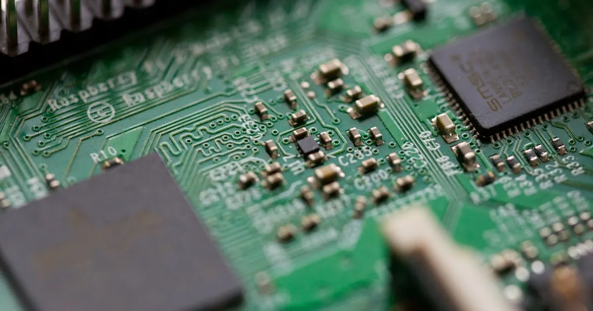
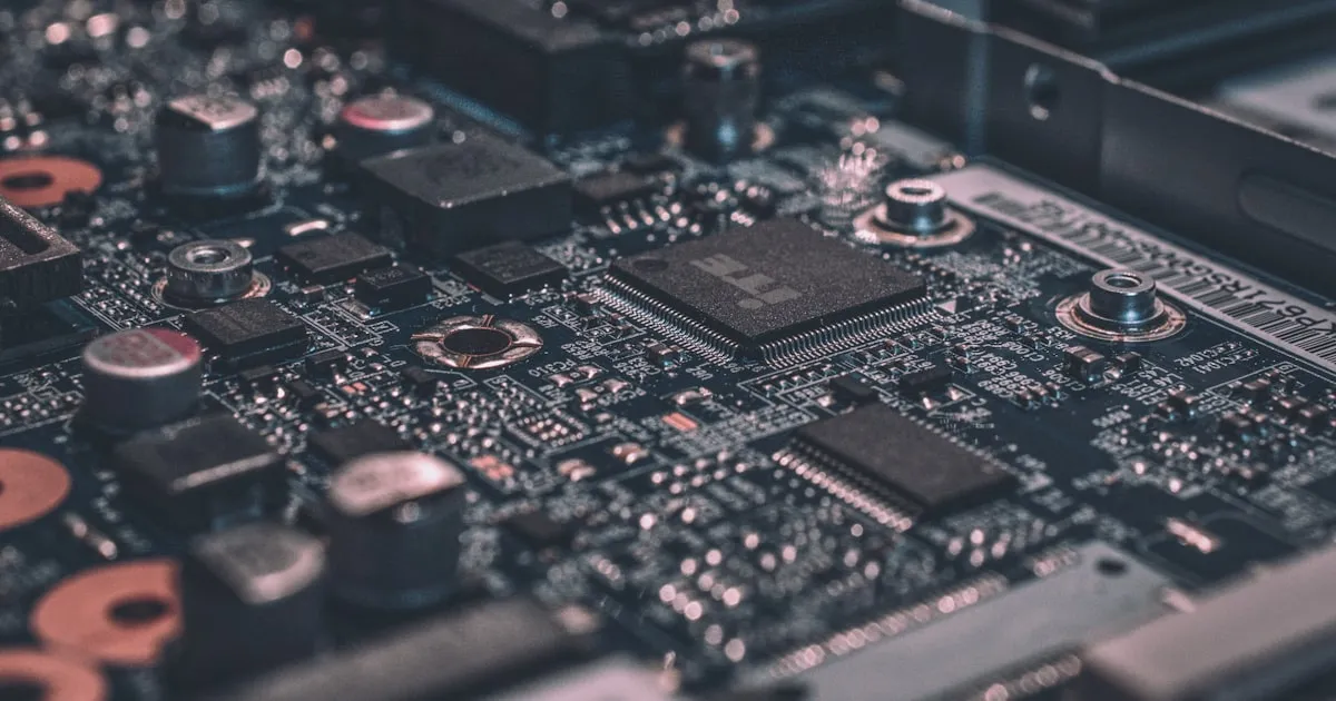
AtlasPCB manufactures RF and microwave PCBs on Rogers, Taconic, and ceramic-filled PTFE substrates with precision thermal via arrays and embedded copper coin technology for GaN power amplifier applications.
IMS 2026 Overview
The International Microwave Symposium 2026 runs June 7-12 in Boston and features:
- 600+ technical papers on RF/microwave/mmWave technology
- Exhibition hall with 500+ companies
- Focus areas: 5G/6G infrastructure, satellite communications, automotive radar, defense electronics
- Co-located: RFIC Symposium and ARFTG Conference
American Standard Circuits (Booth 23056) and multiple other PCB and assembly suppliers are also exhibiting, reflecting the growing intersection of PCB manufacturing capability and RF system performance.
Further Reading
- RF PCB Design: Rogers vs PTFE Material Selection for 5G
- PCB Thermal Via Array Design for High-Power Applications
- PCB Copper Coin Thermal Management for High-Power Components
Image: Nicolas Thomas via Unsplash
About AtlasPCB — We specialize in complex PCB manufacturing for HDI, RF, and high-reliability applications. Explore our RF and high-frequency PCB services . Every order includes free engineering review. Get your quote.
Reviewed by AtlasPCB Engineering Team — IPC-certified manufacturing specialists with 15+ years of production experience in HDI, RF, and high-reliability PCB fabrication. Content based on factory floor data and real customer design reviews.
- news
- IMS 2026
- die attach
- RF PCB
- GaN
- 5G
- gold-tin solder
- microwave