· AtlasPCB Engineering · News · 3 min read
EV Group Showcases 450nm Pitch Hybrid Bonding and Layer Transfer at ECTC 2026
EV Group (EVG) highlights breakthrough hybrid bonding, IR layer transfer, and maskless lithography technologies at ECTC 2026 — demonstrating 450nm pitch Cu-Cu bonding with 98% yield across 20 million interconnects for next-generation AI chip packaging.
EV Group (EVG), the Austrian semiconductor equipment manufacturer, announced on May 19, 2026 an extensive program of technology demonstrations at the 76th IEEE ECTC conference (May 26-29, Orlando, FL), including a landmark result: 450nm pitch Cu-Cu hybrid bonding with 98% yield across 20 million interconnects — a critical milestone for ultra-dense 3D chip integration powering next-generation AI processors.
Key Technologies Showcased
Ultra-Fine Pitch Hybrid Bonding (450nm)
Co-authored with Applied Materials, EVG demonstrated:
- 450nm Cu-Cu interconnect pitch — among the finest pitches demonstrated at production-scale wafer sizes
- 98% yield across 20 million interconnects — proving manufacturing viability, not just lab results
- Wafer-to-wafer (W2W) process using EVG’s GEMINI® FB production bonding systems
This pitch density enables significantly higher bandwidth die-to-die interfaces than current 2-3μm pitch hybrid bonding used in today’s HBM stacks. For AI accelerators demanding multi-terabyte/second memory bandwidth, sub-micron bonding pitch is the enabling technology.
300nm Pitch Process Integration
A separate paper (co-authored with Applied Materials) presents:
- 300nm pitch hybrid bonding with SiCN passivation
- 50nm overlay accuracy — critical for alignment at these feature sizes
- Fine-grain Cu metallurgy with comprehensive reliability assessment
- Path to production: Demonstrates readiness for upcoming HBM5/6 generations
IR Layer Transfer (LayerRelease™)
Co-authored with imec:
- Fabrication and transfer of fine-pitch redistribution layers (RDL) using Si temporary carriers
- IR laser release approach enabling non-destructive layer separation
- Application: heterogeneous integration of pre-fabricated RDL onto target wafers
Maskless Lithography (LITHOSCALE® XT)
For panel-level packaging:
- Digital lithography patterning of dry film resists
- High aspect ratio Cu pillar applications on 310×310mm² panel substrates
- Co-authored with Asahi Kasei Corporation
- Eliminates mask tooling cost for advanced substrate manufacturing
Seven Technical Sessions at ECTC
EVG’s conference program spans the full range of heterogeneous integration:
- Professional development course: “Wafer-to-Wafer and Die-to-Wafer Hybrid Bonding” (Tue, May 26)
- 450nm pitch Cu-Cu hybrid bonding demonstration (Thu, May 28)
- Fine-pitch RDL layer transfer using IR laser release (Thu, May 28)
- 300nm pitch process integration with SiCN (Fri, May 29)
- Digital lithography on panel substrates (Fri, May 29)
- Epitaxial Ru layer transfer — single-crystal interconnects (Fri, May 29)
- Advanced metrology for chiplet integration with Intel (Thu, May 28)
Why This Matters for PCB and Substrate Manufacturing
While hybrid bonding itself operates at semiconductor scale (nanometer features), its implications cascade into PCB substrate manufacturing:
Substrate complexity increases: As chips integrate more dies through hybrid bonding, the organic substrates connecting these packages to the board must support:
- Higher I/O density → finer pitch BGA and land pad arrays
- Higher power density → improved thermal via arrays and embedded cooling
- Higher signal frequency → ultra-low-loss substrate materials
- Tighter warpage control → precision lamination for flat packages
Interposer manufacturing: Silicon interposers using hybrid bonding require organic substrates with:
- ≤ 2μm surface planarity (for flip-chip attach)
- ≤ 5 ppm/°C CTE-matched materials
- Ultra-fine trace/space (< 30μm L/S) on substrate surface
Panel-level packaging: EVG’s LITHOSCALE maskless lithography for 310×310mm panels aligns with the industry trend toward panel-level fan-out packaging — potentially commoditizing substrate manufacturing at scale.
AtlasPCB’s Advanced Substrate Capabilities
As AI chip packages grow in complexity, the PCB substrates that support them must keep pace. AtlasPCB provides:
- Fine-line etching down to 50μm line/space for advanced BGA substrates
- Controlled impedance for high-bandwidth die-to-board channels
- Thermal management solutions (copper coins, thermal via arrays) for multi-hundred-watt packages
- Low-warpage substrates for flip-chip reliability
Designing substrates for next-gen AI packages? Get a quote → | View capabilities →
Sources: EV Group Press Release, May 19, 2026; IEEE ECTC 2026 Technical Program
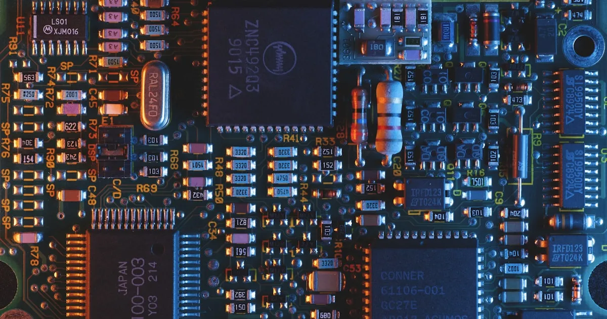
Image: Alexandre Debiève via Unsplash
About AtlasPCB — We specialize in complex PCB manufacturing for HDI, RF, and high-reliability applications. Explore our full PCB manufacturing capabilities, or get an instant online quote . Every order includes free engineering review. Get your quote.
Reviewed by AtlasPCB Engineering Team — IPC-certified manufacturing specialists with 15+ years of production experience in HDI, RF, and high-reliability PCB fabrication. Content based on factory floor data and real customer design reviews.
- news
- ECTC 2026
- EV Group
- hybrid bonding
- advanced packaging
- 3D integration