· AtlasPCB Engineering · News · 4 min read
Electroninks Unveils Air-Curable Copper Ink: Additive PCB Metallization Without Inert Gas
Electroninks announces a breakthrough copper metal-organic decomposition (MOD) ink that cures in ambient air at 150°C, eliminating the need for nitrogen ovens in additive PCB metallization and enabling cost-effective copper patterning on flexible substrates.

Ambient-Condition Copper Metallization Breakthrough
Electroninks, a Texas-based company specializing in metal complex inks for additive manufacturing and semiconductor packaging, has announced an advancement to its copper metal-organic decomposition (MOD) ink platform: a copper metallization technology capable of curing under ambient conditions — open to air, without inert gas infrastructure.
The development, announced in early June 2026, addresses a long-standing limitation of copper ink technology: the requirement for nitrogen or forming gas atmospheres during thermal curing to prevent oxidation.
Technical Details
The new Cu-MOD ink achieves conductive copper film formation through:
- Curing temperature: ~150°C (compatible with most polymer substrates)
- Curing time: 5-10 minutes
- Atmosphere: Open air (no nitrogen, no vacuum, no forming gas)
- No specialty tooling required: No heat press, no lamination, no inert ovens
- Substrate compatibility: Polyimide, glass, epoxy mold compound (EMC), and build-up films
Preliminary results indicate resistivity performance comparable with existing copper metallization approaches, with full performance data expected in Q3 2026.
Why This Matters for PCB Manufacturing
Traditional PCB fabrication creates copper patterns through subtractive processes — laminating copper foil to substrate, then etching away unwanted copper. This generates significant chemical waste and limits pattern resolution to what lithography and etching can achieve.
Additive copper metallization deposits copper only where needed, offering potential advantages:
- Reduced waste — no copper etchant waste stream
- Finer features — inkjet or aerosol printing can achieve < 25 µm line/space
- Substrate flexibility — works on materials that can’t survive conventional lamination
- Lower temperature — 150°C vs. 180-220°C for standard lamination
- Simpler process — fewer wet chemistry steps
The key barrier has been that copper oxidizes instantly at elevated temperatures in air, requiring expensive nitrogen ovens that negate the simplicity advantage. Electroninks’ ambient-cure technology removes this barrier.
Market Applications
The immediate target applications include:
- Semiconductor packaging: Redistribution layers (RDL) on fan-out wafer-level packages
- Flexible electronics: Conductive traces on polyimide and PET substrates
- Display interconnects: Fine-pitch routing on glass substrates
- Repair and rework: Selective copper deposition for PCB repair
- Large-area electronics: IoT sensors, RFID antennas, photovoltaic interconnects
“While silver and gold will remain key materials in many applications, for large-area and full-film metallization, the rising cost of precious metals has renewed interest in cost-effective alternatives,” said Kazutaka Ozawa, Technical Director at Electroninks.
Implications for the PCB Industry
This technology sits at the intersection of several industry trends:
Cost Pressure on Precious Metals
Silver conductive ink (the current standard for printed electronics) has become increasingly expensive as silver prices have risen 40%+ over the past two years. Copper ink at 1/50th the material cost of silver becomes economically compelling for large-area applications.
mSAP and SAP Processes
The semiconductor-inspired modified semi-additive process (mSAP) already uses thin copper seed layers for fine-line HDI. Air-curable copper ink could potentially replace the sputtered or electroless seed layer, simplifying the process chain.
Sustainability
The PCB industry faces growing pressure to reduce chemical waste, particularly from copper etching and wastewater treatment. Fully additive copper patterning could eliminate the etching step entirely for certain product categories.
Current Limitations
Electroninks acknowledges the technology is still in development:
- Partner-only access: Currently limited to select development partners
- Conductivity: Approaching but not yet matching bulk copper (full data in Q3 2026)
- Adhesion: Long-term reliability on various substrates under validation
- Thickness: Current films are thin — multi-pass printing needed for current-carrying traces
- Speed: Print speed vs. conventional panel plating throughput not yet competitive for volume production
What AtlasPCB Is Watching
At AtlasPCB, we’re monitoring additive metallization technologies closely. While conventional subtractive and semi-additive processes remain optimal for current production volumes, ambient-curable copper ink could become relevant for:
- Prototyping rapid-turn boards with fine features
- Selective repair and rework of high-value boards
- Hybrid approaches combining conventional fabrication with additive fine-pitch features
- Future mSAP/SAP seed layer alternatives
Source
Electroninks announcement via PCB Directory, June 2026.
Need cutting-edge PCB fabrication technology? AtlasPCB stays at the forefront of manufacturing innovation, from HDI microvia technology to advanced surface finishes. Get a quote for your next-generation design.
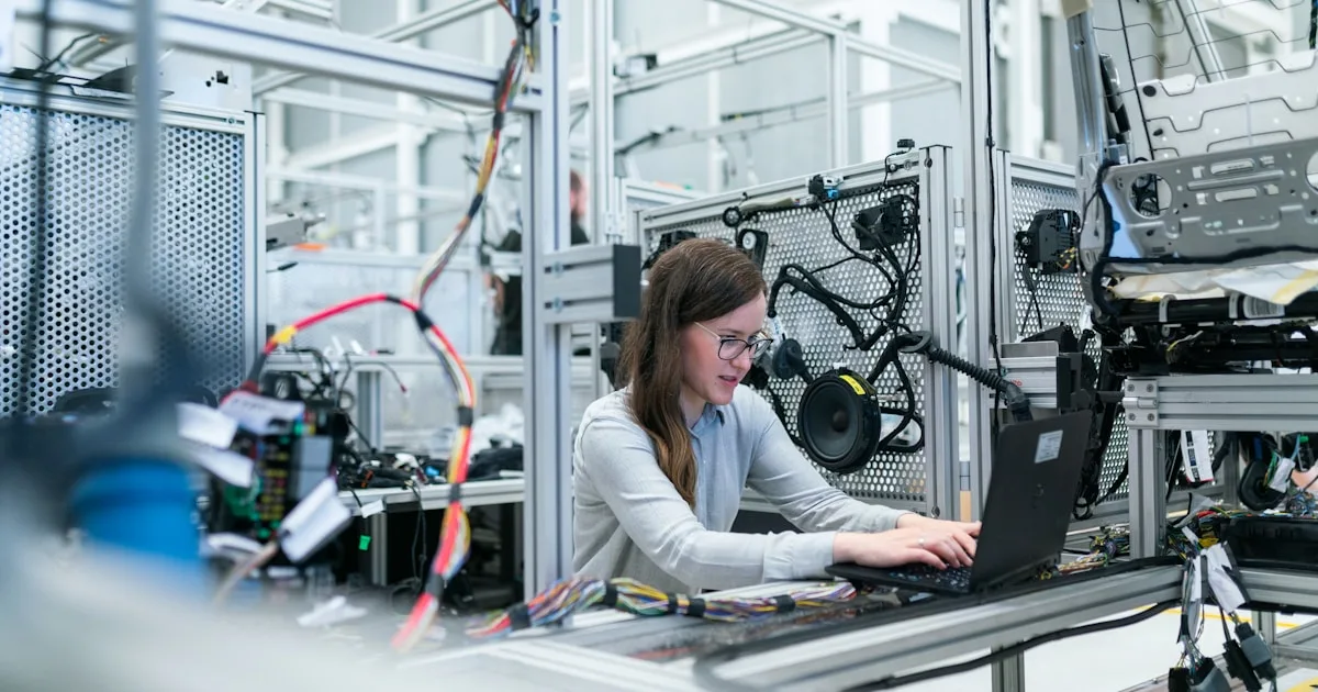
Image: Conductive ink application via Unsplash
About AtlasPCB — We specialize in complex PCB manufacturing for HDI, RF, and high-reliability applications. Explore our full PCB manufacturing capabilities, or get an instant online quote . Every order includes free engineering review. Get your quote.
Reviewed by AtlasPCB Engineering Team — IPC-certified manufacturing specialists with 15+ years of production experience in HDI, RF, and high-reliability PCB fabrication. Content based on factory floor data and real customer design reviews.
- news
- additive-manufacturing
- copper-ink
- pcb-fabrication
- mod
- flexible-electronics
- printed-electronics