· AtlasPCB Engineering · News · 4 min read
The Inference Flip: Edge AI Now Consumes Two-Thirds of Global AI Compute, Reshaping PCB Demand
By mid-2026, AI inference workloads surpass training compute for the first time — driving explosive demand for edge AI PCBs with NPU-optimized stackups, thermal management, and HDI routing that differ fundamentally from data center boards.
Key Takeaway
The “inference flip” has arrived: by mid-2026, AI inference workloads account for approximately two-thirds of all global AI compute, surpassing training for the first time. This fundamental shift is creating massive new demand for edge AI PCBs — compact, thermally optimized boards designed for on-device machine learning that differ substantially from the data center backplanes that dominated AI hardware demand in 2024–2025.
What the Inference Flip Means for PCB Manufacturers
The first wave of AI PCB demand (2023–2025) concentrated on a narrow product category: high-layer-count server backplanes (20–40 layers), advanced packaging substrates for GPUs, and high-speed interconnect boards for data centers.
The inference flip diversifies AI PCB demand across an entirely new product spectrum:
| Segment | Typical Layers | Board Size | Volume/Design | Key Challenge |
|---|---|---|---|---|
| Cloud AI training | 20–40 | 600×450 mm | Low | Signal integrity |
| Cloud AI inference | 14–24 | 300×250 mm | Medium | Power delivery |
| Edge AI (industrial) | 8–12 | 100×80 mm | High | Thermal mgmt |
| Edge AI (consumer) | 6–10 | 40×30 mm | Very high | Size + cost |
| Edge AI (automotive) | 8–14 | 120×100 mm | Medium-high | Reliability |
The volume shift is dramatic: for every cloud GPU board manufactured, hundreds of edge AI boards ship. The PCB industry’s growth is now driven by edge AI volume, not cloud AI ASP (average selling price).
Market Drivers
Why Inference Is Moving to the Edge
Multiple forces are pushing AI processing from cloud to edge:
Economics: Cloud inference costs have reached a tipping point. When cloud costs exceed 60–70% of equivalent on-premises edge hardware over 18 months, the business case for edge deployment becomes overwhelming. For always-on applications (security cameras, industrial sensors), edge AI pays for itself within months.
Latency: Real-time applications (autonomous driving, robotic control, interactive devices) cannot tolerate cloud round-trips. Edge inference provides sub-millisecond response times vs. 50–200ms for cloud.
Privacy: Regulatory pressure (EU AI Act, CCPA, sector-specific rules) increasingly restricts transmitting raw sensor data to cloud. Edge processing keeps sensitive data local.
Reliability: Edge devices continue functioning during internet outages. For safety-critical applications, this is non-negotiable.
AI-Enabled Industrial PCs: 20% Penetration by 2026
The AI Box market — ruggedized industrial PCs with dedicated NPUs — is projected to reach approximately 20% penetration in manufacturing, healthcare, transportation, and energy verticals by year-end 2026. Each unit requires a purpose-designed PCB with:
- NPU thermal management (15–50W in fanless enclosure)
- Multiple high-speed interfaces (PCIe 4.0, USB 3.2, GbE, MIPI CSI)
- Industrial temperature range (-40 to +85°C)
- 10+ year component availability
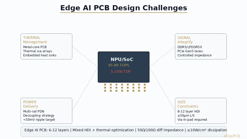
New PCB Requirements for Edge AI
Compared to Traditional Embedded
Edge AI PCBs differ from conventional embedded designs in several critical ways:
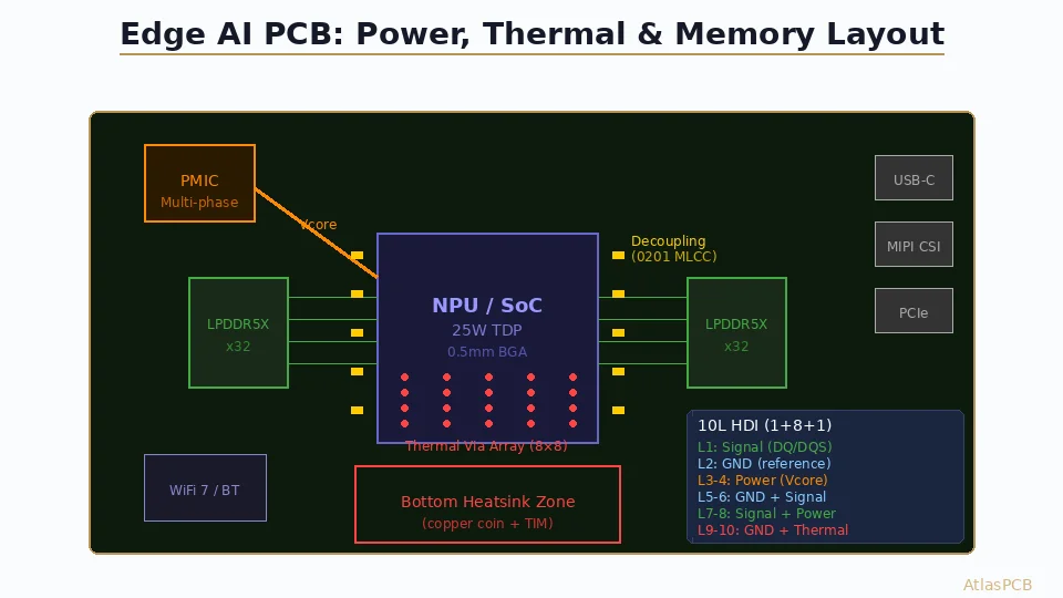
Power delivery: NPUs draw 10–50W with 100A/μs transient response requirements. Traditional embedded processors (Cortex-A class) draw 2–5W with gentle transients. The PDN complexity of edge AI approaches that of desktop PC motherboards — on a board 1/4 the size.
Thermal density: 2–5 W/cm² thermal density from NPU packages requires thermal via arrays, copper coins, or embedded heat spreaders. Standard embedded boards manage < 1 W/cm² with simple copper pours.
Memory bandwidth: LPDDR5X at 8.5 Gbps/pin requires impedance-controlled routing with ±0.5 mm length matching — constraints previously limited to server boards.
HDI requirement: 0.4–0.5 mm pitch BGA packages demand microvia escape routing. Standard PTH PCBs cannot achieve the density required.
Manufacturing Capability Gap
Not all PCB manufacturers can produce edge AI boards. Requirements include:
- Laser drilling capability (microvias)
- Impedance control within ±5% (not the ±10% acceptable for consumer)
- Copper filling for thermal vias (not just plating)
- Sequential lamination for HDI build-up
- Fine-line capability (3/3 mil minimum)
This creates opportunity for manufacturers with HDI and advanced capability to capture the growing edge AI market segment.
What Hardware Engineers Should Know
Design Trade-offs
Edge AI PCB design is fundamentally about managing trade-offs:
- Layers vs. cost: Each additional layer adds 10–15% cost; optimize to minimum viable layer count
- Thermal vs. size: Larger copper area spreads heat better but increases board size
- Performance vs. power: Higher memory bandwidth requires more layers and tighter routing, increasing both cost and power plane complexity
- Volume vs. specification: Consumer edge AI (millions of units) demands ruthless cost optimization; industrial (thousands of units) prioritizes reliability
Getting Started
For teams entering edge AI hardware design:
- Start with module-based solutions (Jetson Orin, Qualcomm RB5) to validate algorithms before custom PCB
- Budget 8–12 layers minimum for any serious NPU-based design
- Engage your PCB manufacturer early — HDI designs benefit from DFM review before layout starts
- Plan thermal solution concurrently with PCB stackup — they’re inseparable
AtlasPCB Edge AI Capabilities
AtlasPCB manufactures edge AI PCBs with:
- 8–16 layer HDI with 1+N+1 and 2+N+2 build-up
- Copper-filled thermal vias (Rth < 1°C/W per array)
- Impedance control ±5% with TDR verification
- Fine-line 3/3 mil on inner layers
- Sequential lamination for complex stackups
Sources: OPD Design “Edge AI and Smart Hardware” (2026); industry analyst estimates; NVIDIA, Qualcomm, MediaTek product roadmaps
Designing an edge AI product? Start with AtlasPCB’s engineering review service — we’ll optimize your stackup for thermal, signal integrity, and manufacturing cost.
Image: Alexandre Debiève via Unsplash
About AtlasPCB — We specialize in complex PCB manufacturing for HDI, RF, and high-reliability applications. Explore our HDI PCB manufacturing capabilities, or get an aluminum and metal-core PCB services . Every order includes free engineering review. Get your quote.
Reviewed by AtlasPCB Engineering Team — IPC-certified manufacturing specialists with 15+ years of production experience in HDI, RF, and high-reliability PCB fabrication. Content based on factory floor data and real customer design reviews.
- news
- edge AI
- inference
- NPU
- PCB demand
- AI hardware
- HDI
- thermal management
- 2026