· AtlasPCB Engineering · Industry News · 6 min read
AI in PCB Manufacturing Goes Mainstream — But Only 10% Have Scaled Deployments
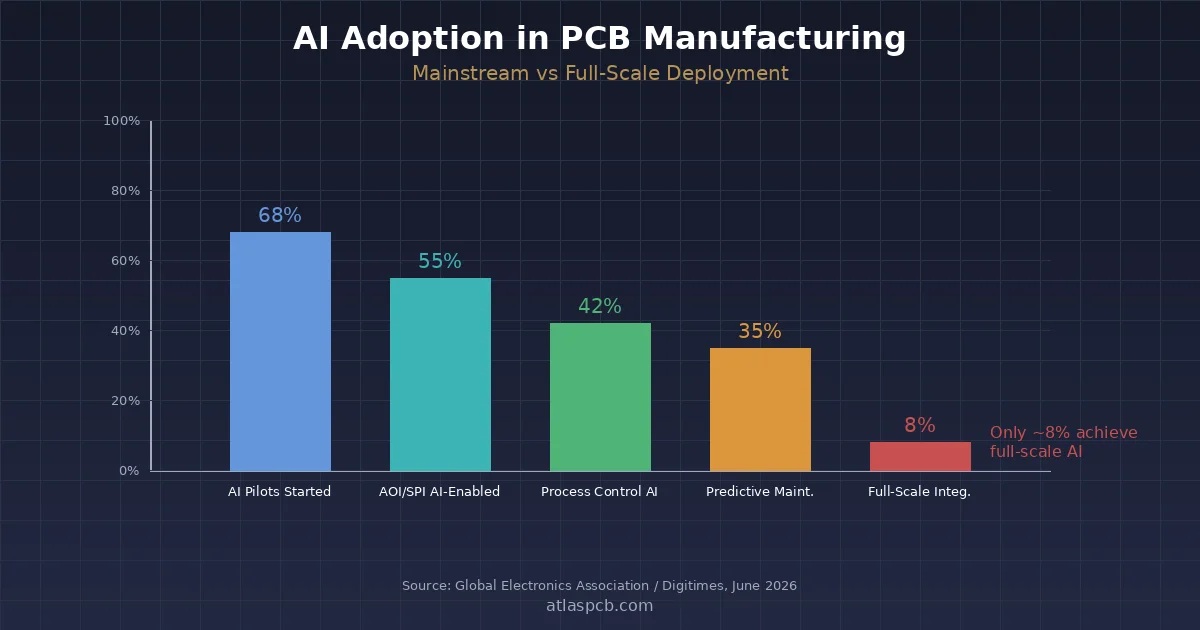
A June 2026 Digitimes report reveals that while AI adoption in PCB manufacturing is now widespread across the industry, fewer than 10% of companies have achieved factory-wide scaled deployments — highlighting the persistent gap between experimentation and production-ready implementation.
AI Adoption Is Universal — But Full-Scale Deployment Remains Rare
A Digitimes industry report published June 10, 2026 confirms what many in the PCB sector already sensed: artificial intelligence has become a standard part of the manufacturing conversation. Nearly every major PCB fabricator globally is running at least one AI initiative. But the report’s critical finding is the gap between adoption and scale — fewer than 10% of companies have moved AI from pilot programs into full production integration across their factory operations.
This 90%+ gap between “experimenting with AI” and “running AI at factory scale” represents the central challenge facing the industry’s digital transformation efforts in 2026.
Key Findings: Where the Industry Stands
The report, drawing on surveys and interviews across Asia-Pacific and North American fabricators, identifies three tiers of AI maturity:
- Tier 1 (under 10%): Full-scale deployment — AI integrated into production workflows, automated decision-making, closed-loop process control
- Tier 2 (approximately 35%): Limited deployment — AI running on specific lines or processes, still requiring human validation for most decisions
- Tier 3 (approximately 55%): Pilot/experimental — proof-of-concept projects, data collection phases, or vendor evaluations
The concentration at Tiers 2 and 3 reflects systemic barriers rather than lack of interest or investment.
Where AI Is Being Applied
AOI and Defect Classification remain the dominant use case, with over 70% of respondents running AI-assisted inspection in some capacity. The value proposition is clear: traditional rule-based AOI generates 15-30% false call rates on complex HDI boards. AI models trained on historical defect data reduce false calls to 2-5% while catching subtle real defects — micro-scratches, partial under-etch, copper roughness anomalies — that rule-based systems miss entirely.
Process Parameter Optimization is the second most common application. AI models correlate input parameters (etch bath chemistry, plating current density, lamination temperature profiles) with output quality metrics to recommend optimal settings in real time. This is particularly valuable for high-mix environments where process windows shift with board complexity.
Yield Prediction models analyze incoming design data and historical production outcomes to flag boards likely to cause yield issues before manufacturing begins, enabling proactive engineering review and process adjustments.
AI-ENHANCED QUALITY
PCBs Inspected by AI-Assisted AOI
Our production lines use AI-assisted defect classification to catch what rule-based systems miss.
Get a Quote ›Why Scaling Remains Difficult
The report identifies three primary barriers to full-scale deployment:
Data Quality and Infrastructure. AI models require clean, labeled, consistently structured data. Most PCB factories have decades of production data locked in disparate systems — MES databases that don’t talk to AOI stations, etch line logs stored in proprietary formats, defect records that lack spatial coordinates. Building the data pipeline is often harder than building the model.
Legacy Equipment Integration. A typical PCB factory operates equipment spanning 5-20 years of vintage. Connecting a 2008-era drilling machine to a modern AI inference pipeline requires custom middleware, sensor retrofits, and protocol translation layers. The cost and complexity of integration compounds with each additional machine type.
Workforce Training. Running AI in production requires operators who understand confidence thresholds, know when to override model decisions, and can identify model drift. This represents a fundamental shift in shop-floor skills that takes 12-24 months to develop across an organization.
What This Means for AtlasPCB and Our Customers
At AtlasPCB, we have integrated AI-assisted inspection into our AOI process for defect classification. Our system is trained on defect libraries specific to the board types we manufacture most frequently — HDI, high-layer-count, and fine-pitch designs — which improves first-pass yield and reduces false escapes reaching our customers.
We are not claiming factory-wide AI transformation overnight. Like the report suggests, responsible scaling means validating each application thoroughly before expanding. What this means practically for engineers ordering boards:
- Fewer escapes: AI catches subtle defects (micro-cracks at via transitions, partial delamination indicators) that would pass traditional inspection
- Faster feedback: When our DFM review flags potential issues, AI-assisted analysis helps quantify the actual manufacturing risk rather than relying solely on worst-case rules
- Consistent quality: AI models do not have bad days, fatigue, or shift-change variability
For deeper context on how AI is changing PCB design verification, see our technical article on AI-powered DFM and machine learning in design rule checking.
MANUFACTURING CAPABILITIES
From 2-Layer to 30-Layer HDI
Advanced fabrication with AI-assisted quality control across all technology levels.
View Capabilities ›Industry Outlook
The Digitimes report projects that the 10% full-scale figure will reach 25-30% by end of 2027, driven primarily by turnkey AI solutions from equipment vendors (embedding inference directly in new AOI and SPI machines) rather than custom in-house model development. This vendor-led approach lowers the integration barrier significantly — factories acquire AI capability as part of equipment upgrades rather than standalone IT projects.
For customers, the bottom line is straightforward: boards manufactured with AI-assisted quality systems deliver measurably lower defect rates. As this technology scales across the industry, the quality floor rises for everyone.
ATLASPCB
Quality You Can Measure
Request a quote and experience PCB fabrication backed by AI-assisted inspection and engineering review.
Start Your Project ›Related Reading
About AtlasPCB — We specialize in complex PCB manufacturing for HDI, RF, and high-reliability applications. Explore our full PCB manufacturing capabilities . Every order includes free engineering review. Get your quote.
Reviewed by AtlasPCB Engineering Team — IPC-certified manufacturing specialists with 15+ years of production experience in HDI, RF, and high-reliability PCB fabrication. Content based on factory floor data and real customer design reviews.
- AI PCB manufacturing
- AOI inspection
- defect classification
- yield optimization
- Industry 4.0
- smart factory
- PCB quality