· AtlasPCB Engineering · News · 5 min read
ABF Substrate Market Hits $7.19 Billion as Advanced Packaging Drives PCB Substrate Boom in 2026
The global ABF substrate market reaches $7.19 billion while substrate-like PCB demand surges to $4.24 billion in 2026. Advanced semiconductor packaging is reshaping PCB manufacturing requirements as chiplets and 2.5D/3D integration demand unprecedented interconnect density.

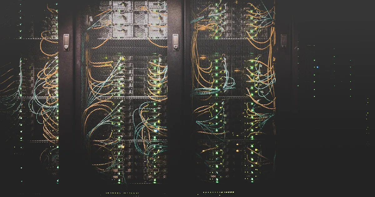
The advanced packaging revolution is rewriting the economics of PCB substrates. New market data shows the ABF (Ajinomoto Build-up Film) substrate market has reached $7.19 billion in 2026, while substrate-like PCB (SLP) demand has surged to $4.24 billion—together representing a fundamental shift in how the electronics industry thinks about interconnect between silicon and system.
Source: Illuminious Market Research and TechInsights 2026 Advanced Packaging Outlook, 2026
What’s Driving the Substrate Boom
The numbers reflect a structural transformation in semiconductor packaging. Three forces are converging to create unprecedented demand for advanced PCB substrates:
1. AI Accelerator Packaging at Scale
Every major AI chip—from NVIDIA’s next-generation GPUs to Google’s TPUs and custom accelerators from Meta, Microsoft, and Amazon—uses advanced packaging that requires the most sophisticated substrates available:
- CoWoS (Chip-on-Wafer-on-Substrate): TSMC’s 2.5D packaging technology places multiple chiplets on a silicon interposer, which mounts on a large ABF substrate. Each CoWoS package requires a substrate costing $80-150.
- HBM integration: High Bandwidth Memory stacks mounted adjacent to compute die on the interposer demand extreme substrate flatness (≤50μm bow) and fine-pitch routing.
- Package sizes growing: Reticle-limit chips (800mm²+) on 2500mm²+ substrates push ABF substrate capabilities to their limits.
2. Chiplet Architecture Adoption
The industry-wide shift from monolithic SoCs to chiplet-based designs multiplies packaging complexity:
- AMD’s Zen architecture: Multiple CPU chiplets + I/O die on organic substrate
- Intel’s Ponte Vecchio/Falcon Shores: 40+ tiles integrated with EMIB and Foveros packaging
- UCIe standard adoption: Universal Chiplet Interconnect Express standardizes die-to-die interfaces, enabling mix-and-match chiplet ecosystems that all need sophisticated substrates
Each chiplet architecture requires more substrate area, more routing layers, and finer features than the previous generation.
3. 5G and Mobile SoC Density
Smartphone application processors at 3nm and below demand SLP or advanced substrate technology:
- Apple A-series and M-series: Fan-out packaging with substrate-level redistribution
- Qualcomm Snapdragon: Package-on-package requiring high-density substrates
- MediaTek Dimensity: Increasingly complex packages for premium mobile tier
The mobile market alone consumes billions of SLP units annually, with each generation requiring finer traces and more layers.
ABF Supply Chain: Still Tight
Despite capacity investments by Ajinomoto (the dominant ABF film supplier) and substrate manufacturers, supply remains constrained:
Ajinomoto’s position: Commands ~80% of the global ABF film market. Their GX-92R and GZ-series films are the industry standard for advanced substrates. Capacity expansions in 2024-2025 added approximately 30% volume, but demand growth has outpaced supply.
Substrate manufacturer capex: Ibiden, Shinko, and Samsung Electro-Mechanics collectively invested over $8 billion in substrate capacity during 2023-2025. Much of this capacity entered production in late 2025 and 2026, partially easing the acute shortages of 2023-2024 but not fully satisfying growing demand.
Lead times: Advanced ABF substrates (4-4-4 build-up or higher, ≤8μm L/S) currently carry 12-16 week lead times for production orders. Standard substrates (12-15μm L/S) have improved to 8-10 weeks.
What This Means for PCB Manufacturers
The substrate boom creates both challenges and opportunities for traditional PCB manufacturers:
Convergence Opportunity
PCB manufacturers with advanced HDI capability are moving toward SLP production:
- AT&S (Austria): Already a major SLP supplier, expanding capacity for Apple and automotive
- Unimicron (Taiwan): Investing in mSAP capability for SLP production
- Zhen Ding Technology (Taiwan): Bridging HDI and SLP for mobile applications
- Shennan Circuits (China): Developing domestic SLP capability
Technology Requirements
To participate in the substrate-adjacent market, PCB manufacturers need:
- mSAP (modified Semi-Additive Process) capability for ≤30μm L/S
- Ultra-thin copper foil handling (1.5-3μm)
- ABF or equivalent build-up film lamination
- Laser Direct Imaging (LDI) at ≤5μm resolution
- Enhanced cleanroom environments (Class 10,000 or better)
- Metrology equipment for sub-20μm measurement accuracy
Material Supply Implications
The substrate boom is creating ripple effects across the entire PCB material supply chain:
- ABF film: Tight supply pushing manufacturers to develop alternatives
- BT resin: Demand increasing for substrate core materials
- Ultra-thin copper foil: Limited suppliers (Mitsui Mining, JX Nippon Mining) face capacity constraints
- Specialty chemicals: SAP/mSAP chemistry requires different plating and etching chemicals than standard PCB production
The Chiplet Economy and PCB Design Impact
As chiplet architectures become mainstream, system designers face new PCB-level challenges:
Package-to-Board Interface Complexity
A chiplet-based processor with 2.5D packaging creates a BGA with:
- 5,000-8,000+ balls
- 0.4-0.65mm ball pitch
- Multiple power domains (>10 voltage rails)
- Signal speeds exceeding 56 Gbps per lane
- Thermal dissipation of 300-600W
The PCB hosting this package must provide:
- Fine-pitch escape routing (requiring SLP or advanced HDI)
- Power delivery with <1mΩ impedance to the package
- Controlled impedance for thousands of differential pairs
- Thermal management (thermal vias, embedded heat pipes)
Multi-Package Coordination
Modern AI server boards host multiple chiplet-based processors, each with its own advanced substrate. The system PCB must:
- Route high-speed links (PCIe Gen6, CXL 3.0, UALink) between packages
- Manage power distribution for aggregate TDPs exceeding 2000W
- Maintain signal integrity across 400mm+ trace lengths
- Handle thermal expansion mismatches between packages and PCB
AtlasPCB Perspective: Serving the Advanced Packaging Ecosystem
While AtlasPCB doesn’t manufacture IC substrates directly, the advanced packaging boom impacts our customers in several ways:
Higher-density main boards: As processor packages use finer-pitch BGAs, the PCBs hosting them need more routing layers and tighter design rules. We’re seeing increasing demand for 16+ layer HDI boards with 50μm trace/space.
Interposer PCBs for test and validation: Semiconductor companies need high-quality test vehicles during package development. These require the same HDI expertise applied to test infrastructure.
System-level thermal management: Advanced packages running at 500W+ need PCBs designed with thermal consideration from day one—copper coin inserts, thermal via arrays, and material selection for high-temperature operation.
Power delivery architecture: Modern processor packages demand <1mΩ PDN impedance, requiring careful PCB stackup design with dedicated power/ground plane pairs and embedded decoupling.
The $7.19 billion ABF substrate market represents the tip of an iceberg that extends deep into traditional PCB manufacturing. Every advanced substrate ultimately mounts on a PCB that must match its performance requirements—creating cascading demand for more capable board-level manufacturing.
Building systems around advanced semiconductor packages? AtlasPCB provides high-layer-count HDI PCBs optimized for fine-pitch BGA escape routing, high-speed signal integrity, and power delivery. Request a quote to discuss your advanced packaging board requirements.
About AtlasPCB — We specialize in complex PCB manufacturing for HDI, RF, and high-reliability applications. Explore our impedance-controlled PCB manufacturing . Every order includes free engineering review. Get your quote.
Reviewed by AtlasPCB Engineering Team — IPC-certified manufacturing specialists with 15+ years of production experience in HDI, RF, and high-reliability PCB fabrication. Content based on factory floor data and real customer design reviews.
- industry news
- ABF substrate
- advanced packaging
- chiplets
- IC substrate
- SLP
- PCB market
- semiconductor packaging