· News · 3 min read
PCB Market to Reach $182 Billion by 2036 as LPKF Unveils In-House Multilayer Manufacturing at Embedded World 2026
The global PCB and PCBA market is projected to grow at 5.1% CAGR reaching $182.2 billion by 2036, while LPKF demonstrates rapid prototyping capabilities that could reshape how engineers approach early-stage PCB development.
The printed circuit board industry continues its steady upward trajectory, with new market research projecting the combined PCB and PCBA market will reach $182.2 billion by 2036, growing at a compound annual growth rate of 5.1%. The forecast, published in April 2026, reflects sustained demand from AI infrastructure, electric vehicles, 5G/6G telecommunications, and aerospace defense programs.
LPKF’s Embedded World 2026 Demonstration
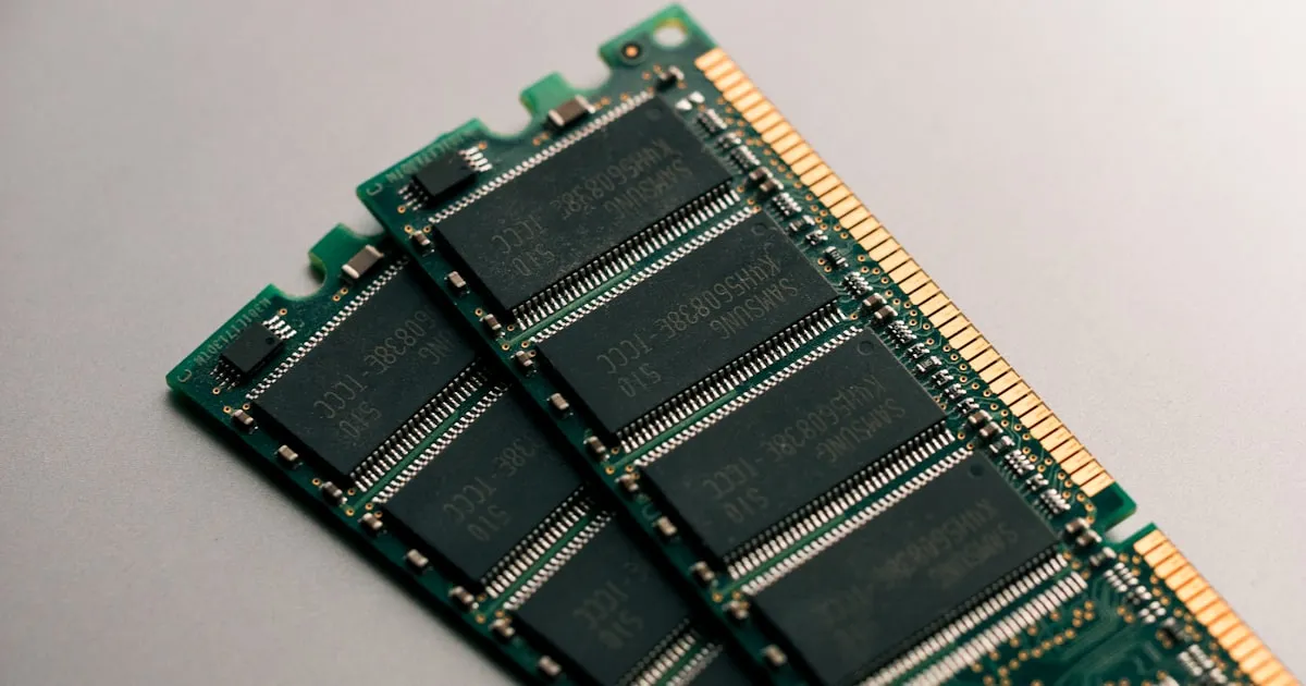
At Embedded World 2026 in Nuremberg (March 2026), LPKF Laser & Electronics SE presented what it calls a “complete workflow for in-house multilayer PCB manufacturing.” The demonstration showcased the company’s ProtoLaser and ProtoMat systems working together to produce functional multilayer PCBs entirely within an R&D lab environment.
The system targets engineering teams that need rapid iteration on 2-4 layer prototypes without waiting for external fabrication turnaround. LPKF claims the workflow can produce a functional 4-layer prototype in under 8 hours — a significant reduction compared to even the fastest quick-turn PCB services.
What This Means for the Industry
For Engineers
In-house prototyping tools are compelling for the first 1-5 iterations of a design where speed matters more than production-quality finish. However, these tools have inherent limitations:
- Layer count: Practical maximum of 4 layers (vs. 30+ from professional fabs)
- Trace/space: Typically limited to 100µm (4 mil) minimum (vs. 50µm from advanced fabs)
- Surface finish: Basic tin plating only (vs. [ENIG, HASL, OSP, and other options]/blog/pcb-surface-finish-enig-hasl-osp-hard-gold-enepig-en/))
- Via quality: Mechanical drilling only, no [laser-drilled microvias]/blog/pcb-laser-drilling-microvia-technology-en/)
- Impedance control: Limited dielectric thickness accuracy
For PCB Manufacturers
The growth of in-house prototyping doesn’t threaten production PCB manufacturing — it accelerates it. Engineers who can iterate faster in-house tend to reach production-ready designs sooner, generating manufacturing orders faster.
The real opportunity for manufacturers lies in the transition from prototype to production. Engineers need a fabrication partner who can take their proven concept and scale it with proper [multilayer manufacturing processes]/blog/multilayer-pcb-manufacturing-process-explained-en/), controlled impedance, and production-grade reliability.
Market Growth Drivers
The 5.1% CAGR through 2036 is driven by several converging trends:
- AI data center expansion: Each GPU server rack requires 50-100+ high-layer-count PCBs with advanced materials
- Electric vehicle adoption: EV powertrains use 2-3x more PCB area than ICE vehicles
- 5G/6G infrastructure: Base stations and small cells require [RF-grade materials]/blog/high-frequency-pcb-substrate-selection-dk-df-en/)
- Aerospace and defense: Geopolitical tensions driving domestic PCB reshoring programs
- Medical devices: Wearable and implantable electronics requiring [specialized manufacturing]/blog/medical-pcb-manufacturing-requirements-en/)
AtlasPCB Perspective
While in-house prototyping tools serve early R&D needs, production designs require the precision, material variety, and quality systems that only professional fabrication delivers. AtlasPCB supports the full spectrum — from quick-turn prototypes (5-7 day turnaround) to high-volume production — with engineering review at every stage to catch DFM issues before they become production defects.
For teams evaluating their prototype-to-production workflow, request a quote to see how our engineering review process can accelerate your transition from lab to production.
About AtlasPCB — We specialize in complex PCB manufacturing for HDI, RF, and high-reliability applications. Explore our full PCB manufacturing capabilities, or get an instant online quote . Every order includes free engineering review. Get your quote.
Reviewed by AtlasPCB Engineering Team — IPC-certified manufacturing specialists with 15+ years of production experience in HDI, RF, and high-reliability PCB fabrication. Content based on factory floor data and real customer design reviews.
- industry news
- PCB market
- LPKF
- rapid prototyping
- embedded world 2026